
I was extensively quoted in the following article by Ann Steffora Mutschler & Ed Sperling. I thought I would pass along a link to it:
All posts by Chris
Goodbye, SEMATECH
In August of 1990 I joined SEMATECH for a one-year assignment that, among many benefits, brought me to Austin. In those days, SEMATECH was a great place to work, full of energy and promise (and yes, too much politics as well). The pre-competitive research consortium wasn’t very efficient at spending money to make a difference, but it most definitely made a difference. It was what the US industry needed at a time of competitive uncertainty, and it attracted some really great people working in a uniquely collaborative environment.
Ten days ago SEMATECH announced its own dissolution, as it merges with SUNY Polytechnic Institute in its new home in Albany. It saddens me to say that my first thought at hearing this news was “ten years too late”. While SEMATECH was the right organization at the right time in the 1990s, it lost its way in the 2000s and never recovered. As the semiconductor industry, and the world, changed to be more global, SEMATECH’s original mission of shoring up the US semiconductor industry became obsolete. But instead of recognizing its fading value, SEMATECH proved the first law of organization: organizations strive first and foremost for the survival of the organization. With all due respect to the many good people that worked there over the years (and still do today), the survival of SEMATECH became the primary goal of SEMATECH, with helping the semiconductor industry a distant second. They left Austin in 2010 chasing money that the State of New York dangled in front of them, and completed their slide into irrelevance.
So, it is with decidedly mixed feelings that I say goodbye to SEMATECH. The last decade has been one of lost opportunity for the organization, but their accomplishments over the years are worth remembering. Mostly, though, I’ll remember the many good people, and good friends, that SEMATECH brought my way.
Salute.
100 Years Ago – an Anniversary of Genocide
100 years ago today marked the beginning of the first genocide of the 20th century – the systematic annihilation of between 1 and 1.5 million Armenians at the hands of the Ottoman empire. Eight years ago I wrote a short essay on why remembering this massacre is important. The message is worth repeating.
Moore’s Law turns 50
On April 19, 1965 Gordon Moore published a paper in Electronics magazine entitled “Cramming more components onto integrated circuits“. Thus was born Moore’s Law, an observation that has driven the semiconductor industry ever since.
I have written a piece for IEEE Spectrum magazine that discusses the history of Moore’s Law and celebrates its impact on our industry, and the world. You can find that article online here:
International Pi Day
What better way to spend this year’s unique international pi day (3.14.15, preferably at 9:26:53 AM) than to go to the world’s most famous circle.

Chris Mack celebrates international pi day at Stonehenge
OK, truth be told this was Sunday morning, the 15th, but it was still pi day in Hawaii, so I’m counting it. The t-shirt proves my nerd bonafides. For a full description of the day, check out my wife’s blog: lippsmackadventures.blogspot.com.
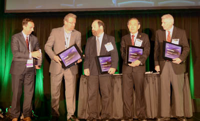
Awards from the SPIE Advanced Lithography Symposium
Here is a recap of the various people who were recognized with awards at this year’s SPIE Advanced Lithography Symposium. (photos by SPIE, http://spie.org/x112637.xml)
Career Achievement Award
Andy Neureuther and Bill Oldham were acknowledged for their “career long contribution to the art and science of lithography.” The award was made “in deep appreciation for your 40 years of visionary guidance and dedication to SPIE society and lithography community.”

12th Frits Zernike Award
Ralph Dammel, CTO of AZ Electronic Materials

Fellows of SPIE
Luigi Capodieci, Bernd Geh, Moshe Preil, Masato Shibuya, and Obert Wood
From the Metrology conference:
Diana Nyyssonen Award for Best Paper in Metrology (2014 conference):
“10nm three-dimensional CD-SEM metrology”, András E. Vladár, John S. Villarrubia, Jasmeet S. Chawla, et al.,
Karel Urbanek Award for Best Student Paper (student lead author at this year’s conference):
“Mechanical and thermal properties of nanomaterials at sub-50nm dimensions characterized using coherent EUV beams”, Kathleen M. Hoogeboom-Pot, Jorge N. Hernandez-Charpak, Travis Frazer, Xiaokun Gu, Emrah Turgut, Univ. of Colorado at Boulder; Erik H. Anderson, Weilun L. Chao, Lawrence Berkeley National Lab.; Justin M. Shaw, National Institute of Standards and Technology; Ronggui Yang, Margaret M. Murnane, Henry C. Kapteyn, Damiano Nardi, Univ. of Colorado at Boulder
From the Patterning Materials conference:
C. Grant Willson Best Paper Award (2014 conference):
“EUV Resists based on Tin-Oxo Clusters”, Brian Cardineau, Ryan Del Re, Hashim Al-Mashat, Miles Marnell, Michaela Vockenhuber, Yasin Ekinci, Chandra Sarma, Mark Neisser, Daniel A. Freedman, and Robert L. Brainard
Hiroshi Ito Memorial Award for the Best Student Paper (2014 conference):
“An insitu hard mask block copolymer approach for the fabrication of ordered, large scale, horizontally aligned, Si nanowire arrays on Si substrate”, Tandra Ghoshal, Ramsankar Senthamaraikannan, Matthew T. Shaw, Justin D. Holmes and Michael A. Morris
Jeffrey Byers Memorial Best Poster Award (2015 conference):
“EUV Resists Comprised of Main Group Organometallic Oligomeric Materials”, James Passarelli, Brian Cardineau, Ryan Del Re, Miriam Sortland, Michaela Vockenhuber, Yasin Ekinci, Chandra Sarma, Mark Neisser, Daniel A. Freedman, and Robert L. Brainard
From the Design Process Technology Co-Optimization conference:
First Annual Franco Cerrina Memorial Best Student Paper Award (2015 conference):
“Toplogy and context-based pattern extraction using line-segment Voronoi diagram”, Sandeep K. Dey, Univ. della Svizzera Italiana (Switzerland)
From the Optical Lithography conference:
Cymer Best Student Paper Award (2015 conference):
“Characterizing the dependence of thick-mask edge effects on feature size and illumination angle using AIMS images” Aamod Shanker, Andrew R. Neureuther, Laura Waller, Univ. of California, Berkeley; Martin Sczyrba, Advanced Mask Technology Ctr.; Brid Connolly, Toppan Photomasks
350 Years of Scientific Journals
On March 6, 1665 something quite special happened. It probably didn’t seem that special at the time, but the publication of the first issue of the Philosophical Transactions in London created a vital communication tool in science: the scientific journal. 350 years later that journal is still being published, joined by tens of thousands of other scientific journals that chronicle and transmit that vital currency of science: knowledge.
I recently wrote a short article on the 350 history of scientific journals. If you are interest, you can find it here.
SPIE Advanced Lithography Epilogue
I gave three talks at last week’s SPIE Advanced Lithography Symposium, and I’ve spent a fair part of this week finishing up the papers. I am happy to say that they are all now complete. As usual, they are available for download for anyone interested.
But I’ve done something different this year. I have, after the fact, recorded my presentations and uploaded them to YouTube. So, for anyone who missed my presentations and wants to hear what I have to say, you can find both the written papers and the talks here:
SPIE Advanced Lithography 2015 – day 4
On Thursday I was EUV focused. My first complaint is that there were too many ASML papers. Of course, this is not ASML’s fault. They are doing most of the important work in this field. Still, some sessions started to feel like an ASML meeting rather than an SPIE meeting.
The first session was directed to high numerical aperture (NA) designs for EUV, and the ASML/Zeiss anamorphic imaging approach looks like a good idea. Current lens designs can’t scale to NA > 0.5 because they result in angles hitting the mask on the order of 9° rather than the current 6°. These higher angles degrade imaging performance, removing most of the advantage of the higher NA. Higher magnification (8X) would fix this, but would result in either much larger mask sizes (an unlikely scenario) or much smaller field sizes (1/4 to be specific). The smaller field size would hit EUV where it hurts most: throughput.
The Zeiss/ASML solution is to have an 8X magnification in the direction needed to lower the incident angles on the mask (the scan direction), keeping the magnification 4X in the slit direction. This results in field sizes 1/2 of the current size, a more manageable problem. And by moving to a design with a central obscuration, the angles on the mirrors are reduced as well, increasing mirror reflectivity and overall optics transmission. To keep the projector at six mirrors, the higher NA will require extreme aspheres, a daunting manufacturing challenge. But as Bernhard Kneer of Zeiss said, in perfect Teutonic style, “Zeiss can do this.” I love it.
I’m pleased to see ASML acknowledge that higher resolution will require higher dose for EUV. They projected a need for 60 mJ/cm2 for 8-nm half pitch. They are also beginning to grapple with the hard problem of stochastics, framing the issue as an overlay (or edge placement) problem rather than a CD control (LWR) problem. An afternoon talk by Jan Mulkens provided a scenario where edge placement errors caused by stochastics were about of equal magnitude as those caused by overlay errors. I agree that this is a very valuable way of looking at the problem.
I did manage to sneak out of the EUV sessions to visit the world of DFM (design for manufacturing) and hear Andrew Burbine of Mentor talk about the Akaike Information Criterion for evaluating model performance. Finally! I teach about this criterion, as well as other model evaluation criteria, in a statistics course I give at the University of Texas. It is quite standard practice in many fields of model calibration, and is taught as a best practice in most textbooks on the topic. It is good to see it come into the field of OPC model calibration. Kudos to Mentor. Now if they can just get their customers to think about such metrics, as well as 4-fold validation, as better judges of model quality than just RMS fit error.
I have a new award: for the talk with the best last-minute title change. From Imec,
Original title: “No More of Moore’s Law: the high cost of dimensional scaling”
New title: “Maintaining Moore’s Law: enabling cost-friendly dimensional scaling”
Do you think an angry boss might have been involved in this change of heart?
Here is my summary of the reported progress in EUV. ASML rolled out their 40W source to the NXE:3300s in the field last year, and it is now the standard source for most of those users. TSMC got the first 80W source late last year, and that tool is operating mostly as expected, but with only 55% availability. The result is about 40 wafers per hour using a 23.5 mJ/cm2 dose. Cymer has shown a bench source operating at 110W for one hour, but the much anticipated 250W source is still a long ways away. I suspect we’ll see a 100W source in the hands of a customer by the end of the year.
This is good progress. Is it enough? Everyone admits that EUV has missed the window for insertion at 10 nm (except maybe the investor relations team at ASML). What will it take to have EUV established as the plan of record for 7 nm? It will take even faster progress this year. I wish the hard working folks at ASML good luck.
Many people ask me what the most exciting or revolutionary idea was this year at SPIE. But that is not really the point. Sure, every now and then some really new idea seems to come out of nowhere and take off. I first mentioned in my 2010 conference blog that DSA was starting to look less like a science project and more like a technology. But it is the accumulation of progress on DSA over the last 5 years that is the real story. And this year is like most years: a year of incremental progress. Like Moore’s Law itself, where 50 years of incremental progress have resulted in revolutionary changes in capability, our incremental progress is best viewed as accumulated progress. We push hard every year, and over the years the change is absolutely remarkable. I enjoyed watching that progress reported here this week. And I’m sure I’ll enjoy it even more next year.
SPIE Advanced Lithography 2015 – day 3
When you walk into conference room 220A, it will be under the watchful eyes of the “lithography luminaries”. These life-size posters of people who have made out-sized contributions to lithography are part of SPIE’s celebration of the International Year of Light. Some are a sampling of the great scientists who contributed to optical science and technology: Lord Rayleigh, Ernst Abbe, Frits Zernike. The rest are a sampling (of course, incomplete) of folks who have contributed directly to semiconductor lithography. I’m proud (and a tad embarrassed) to be among them. And then someone pointed out the hyphen. I guess one should always be mindful of one’s mortality (Chris Mack, 1960 – …).
I spent the morning of day three learning about progress on directed self-assembly (DSA). Defectivity levels are below 1/cm2, a major milestone but still too high. DSA for contact hole shrinking and uniformity enhancement seems very close to mature enough for manufacturing. Is it ready? I wish that more manufactures were here giving papers talking about their progress in this and other areas. Samsung is conspicuous in its relative absence. On the other hand, Intel, a company that perennially listens more than it talks, is much better represented this year than in the past.
DSA for lines and spaces still needs work. It is interesting to see that line-edge roughness is one of the big problems for DSA, since we all thought that low LER would be one of its major advantages. It doesn’t help that its competitor is SAQP (self-aligned quadruple patterning), a technique with about the lowest LER possible. Comparisons of DSA to SAQP will determine if DSA is ready for manufacturing, both in terms of performance and cost. It is getting close. Dan Millward of Micron reported on Monday that it is only 10% away on the LER metrics.
I also heard some competing exercises comparing the impact on design of choosing SAQP or EUV for the 7nm node. Lars Liebmann showed some standard cells designed making assumptions about the restrictions that SAQP and EUV would impose, then found that routing would be impacted the most, with EUV having an area advantage. Julien Ryckaert of Imec should that a clever introduction of an extra middle of the line (MOL) metal layer, as well some other optimizations, could eliminate the area penalty of using SAQP. The Liebmann and Ryckaert studies were complimentary, and more of these exercises are certainly necessary to understand the impact of lithography on 7nm-node design.
In the afternoon I heard about the progress of multi-electron beam tools. IMS Nanofabrication talked about the most promising application of multibeam writers: mask making. Their tool has made it through the alpha stage and they are hoping to have a production instrument in 2016 (despite having “Ready for Use” in the title of their talk). Mapper seems to continue its trend of pushing out their schedule by one year every year. Still, if they can demonstrate one wafer per hour in the next year or two, that will be a major milestone worth celebrating. The REBL program was dropped by KLA-Tencor in the past year, but it seems that TSMC has not given up on it. It will be interesting to see if TSMC can find another supplier to pick up that technology.
At the poster session I was very pleased to see the posters much more spread out than in years past – thank you SPIE! It was very pleasant to mingle and talk to authors with an adequate amount of room.
After a sampling of wonderful hospitality suites (thanks to the vendors who let me in despite that I will never buy their products), I ended the evening at the PROLITH party. It was 30 years ago that I gave my first talk at this conference (“PROLITH: a comprehensive optical lithography model”). Of course, I had no idea that this paper would have such a momentous impact on my life. It has been a great 30 years, and I am grateful for all the friends I have made in this community. It was also 30 years ago that I held the first bathtub party. (If you don’t know what that means, you can read some of my past blogs from this conference here). I was very glad to end the evening carrying my 30th anniversary PROLITH beer glass.