
In years past, the annual SPIE conference on photomask technology (referred to as BACUS by us old-timers) included an entertainment program with insider jokes and songs from industry folks (who called themselves “Bacchanalians”). The conference was all online this year, so some of the Bacchanalians made of few videos in the spirit of the BACUS entertainment. Thanks to Any Neureuther, Bryan Reese, and Tony Vacca for giving us something to smile about, and for reminding us of the long tradition of fun we had at the BACUS Entertainment.
Category Archives: General
Items that do not fit in other categories
What I do when I’m bored during lockdown
Another day, another Zoom meeting. What can you do to relieve the boredom (not to mention the stress)? This is what I do – make a music video:
I hope it brings a smile, and feel free to share.
Where I am NOT this week
Like most people, I am at home this week. Where I am NOT is New Orleans, attending the 3-beams conference (EIPBN, the Electron, Ion, and Photon Beam Technology and Nanofabrication conference), which has been canceled this year. To see where I hope to be this time next year, this is how the conference chairs announced the venue for 2021:
Solar Panels, Year 3
Here is another annual update on my solar production and electricity consumption. In late January, 2017, I turned on my new solar panels. I have 30 panels, 320 W each, for a total capacity of 9.6 kW (LG320 NeON2 MonoX Plus panels with microedge converters). In the first year I generated 96% of the electricity I consumed (a magical year, with near perfect weather – sunny, but not too hot). The second year was not as good since my consumption went up 6% and my generation was down 10%. The result was that my panels generated 81% of my usage for the second year. The third year is off a little more. My consumption when up 1.5%, and my generation was down 5% compared to the second year. The final result is that the panels generated 76% of my usage in the third year. The weather is the biggest variable, and I need to find an authority that measures the amount of sunshine in Austin so that I can try and determine if there are any other factors than that at play.
COVID-19: the data
Like almost everyone else, I am now hunkering down in my house doing the “social distancing” thing. Since the announcement of the first confirmed coronavirus cases in Austin Thursday night (less than four days ago), events have been accelerating almost as fast as the virus has been spreading. My kids are on Spring break, but I doubt they will be going back to school next week. The supermarket shelves are getting bare. I work from home anyway, so that is no change for me.
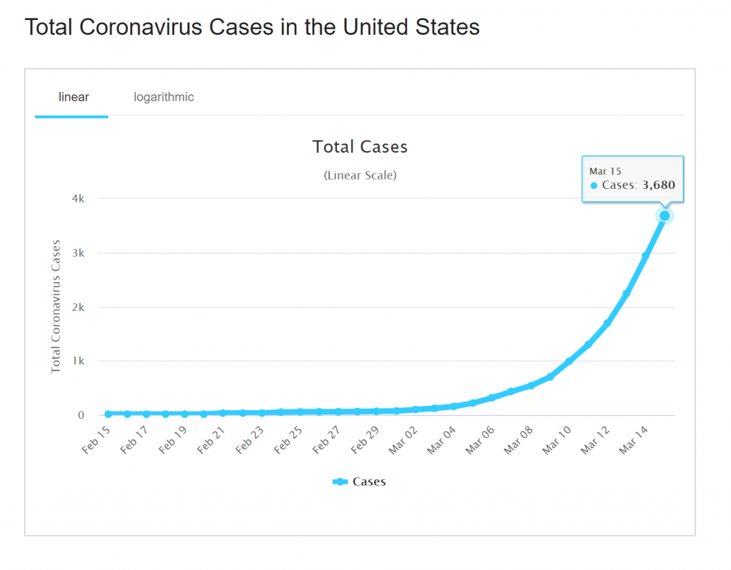
Like everyone else, I am consuming the news about the spread of this disease. But as a data geek, I want more than what you find in the newspapers (yes, I’m old school – news is something you read, not something you watch). The first obvious place to go is the CDC website. Their data is perhaps the most trustworthy, but also conservative and a few days old. There is also the more accessible Worldometers site, with very up-to-date numbers that may be less reliable than the CDC (though I am not diving into that). Below are a couple of links and graphs from those sites. The bottom line: the number of cases in the US seems to be doubling every four days. That’s a 10X increase every two weeks. Exponentials – yikes. If we don’t flatten this curve, that will mean 400,000 cases in a month, and the entire country in two months. It is time for us to flatten the curve.
https://www.worldometers.info/coronavirus/country/us/
https://www.cdc.gov/coronavirus/2019-ncov/cases-updates/world-map.html
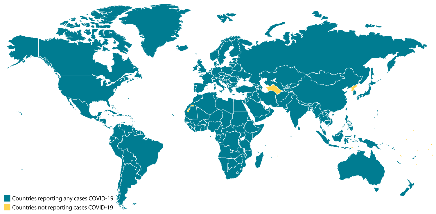
(Countries with coronavirus cases shown in green, as of March 14.)
Quitting Your Job: How Hard Could It Be?
Almost everyone has had the experience of quitting a job. It’s not that hard. You just go to your boss and say “Take this job and … find someone who will better appreciate its benefits.” But things are more complicated when that job is with the National Security Agency.
I joined NSA at Fort Meade, MD as my first job out of college, and worked there for nine years in the 80s and early 90s. (These were the good old days of NSA, before they started spying on Americans.) I was very proud of my work there, making semiconductor encryption chips. Like most of the people there, I had the highest security clearance the government offered – Top Secret Special Intelligence. We scoffed at those piddly Top Secret clearances that they gave away like candy over at the CIA – this was the real deal. And when you agree to accept this clearance there are certain freedoms you voluntarily give up.
The most obvious freedom I gave up was being able to talk about my work. I could only talk about work at work, and outside of work I would end up talking about the people at work, which is more interesting anyway. But the strangest lifestyle difference was the inversion of what is private and what is public. Work became private, and my personal life could only remain private if it was boring. The security office at NSA worried about its employees being blackmailed, so the skeletons in each of our closets were actively exhumed through regular security reviews and polygraph tests.
In 1988 an organization called SEMATECH was started up in Austin, Texas. For those of us working in chip manufacturing, this was a big deal – a consortium of the largest US semiconductor companies, Intel, IBM, Motorola, sending people and money to this new research lab, with the Department of Defense contributing 50% of the budget. It was the cutting edge of my profession. So I thought, maybe I could get assigned to SEMATECH for a year or two to work with these great people doing important research in the interest of US security. And moving from Baltimore to Austin for a while could be fun. Everyone at NSA agreed this would be a great idea, but there was one problem: it had never been done before. And the first rule of bureaucracy is “If it’s never been done before, it can’t be done.”
Bureaucrats have a bad reputation, mostly undeserved since they are the people that actually get things done in government. After all, the other group of government employees is politicians, and we know how much good they do. Government employees operate under an important constraint that most people don’t realize. At your job, you have rules, and if you break those rules you get in trouble, unless breaking the rules makes your company a lot of money, and then you get a pat on the back and a promotion. But in the government these rules go by a different name: they’re called laws. You don’t just break the rules, you break the law. A guess what – government employees don’t like breaking the law, so they work very, very hard to make sure everything they do follows the huge and continuously growing set of regulations that apply to almost everything they do.
It was hard to figure out how to make the regulations work so that I could be temporarily assigned to SEMATECH, but I was determined, and I was a pretty good bureaucrat. Through a lot of careful study of regulations and a lot of advocacy from my boss and my boss’s boss and my boss’s boss’s boss and a team of people from finance and legal at NSA, we created a plan and made it work. I left Maryland to come to Austin to work at SEMATECH. It was great! I did cool work with cool people, I wrote and published papers and presented at conferences, and we made a real difference. And when my 16 month assignment was over, I decided I couldn’t leave. I had fallen in love with Austin. I had found my home. So six weeks before I was supposed to go back, I told my boss I was going to resign. Of course, she was disappointed, but she understood my decision.
For my last week of working for NSA, I flew back to Maryland and started the week-long debriefing process. Quitting a job with a TSSI clearance is a lengthy process. On Monday and Tuesday it was meetings with my boss and group about projects and hand-offs, cleaning out my desk, all the normal stuff. On Wednesday I got the library to sign off that I had no overdue books. On Thursday I went to finance to finish up with my final paycheck and expense reports and to get their sign-off before the final security debriefing on Friday. And this is where things went horribly wrong. When I handed finance my exit form for their signature, they said “Sorry, we can’t sign this because our records show you owe us for an expense overpayment we made. Once you write us a check for the overpayment we can sign your form.” Well that’s odd, I thought, but OK. “How much do I owe?” “$120,000.”
What?!?!? $120,000? That was more than two years of my salary!
There must have been a mistake. No, they assured me that they had been working on these calculations for over a week, all the numbers had been double checked and approved, and they had applied the rules pursuant to joint federal travel regulation §301-74.24 scrupulously.
Regulation 301 what?
They explained to me what this regulation meant. Suppose you are on a TDY (that’s Temporary Duty, government speak for a business trip) and you fail to meet your obligations of the TDY. For example, you are sent on a trip to attend a conference but instead you go to the beach all week. The government can require reimbursement of their expenses in sending you on the trip, including your salary for the week. I was on an extended TDY, and the claim was that my obligation for the 16 month trip was to bring everything I had learned at SEMATECH back to NSA for use there, and by not returning it was the same as if I had spent 16 months at the beach instead of working.
I knew this could not possibly be right, but I discovered that finance was just doing what they were told. My boss’s boss, who had gone to the mat two years before to figure out how to send me to SEMATECH, was pissed! He had written a memo to finance the week before invoking this regulation, and the bureaucratic wheels had begun to spin. It didn’t matter that I was being crushed under them. I tried to call him, my new nemesis, but he refused my calls. I went to his office but a security guard was stationed there to keep me out. That night I was angry, but also determined. I would fight this, lawyer up if needed. I was obviously in the right, and I was not about to let some petty paper pusher ruin my life.
On Friday I went to my all-day security debriefing. At the end of the day I handed my exit form to the security officer for that final signature. “I can’t sign this,” he said. “It’s not signed by finance. They have to sign it first before I can sign.” OK. But what does that mean? “It means you can’t resign.”
Can’t. “Can’t,” he said. I can’t quit my job. That was a thought that had never occurred to me. My first reaction was, “Oh yeah, watch me.” I’ll just leave and never come back. What’s that if not quitting?
But then the security officer said four words that froze me in my tracks: “The 59 minute rule.”
I’m guessing none of you know what the 59 minute rule is, but I knew perfectly well what he meant. In the 1960s two NSA mathematicians had gone on vacation together for a week. On the following Monday they didn’t show up for work. Their boss was surprised, but assumed they had just decided to extend their trip. The next day goes by, and then the next. They still don’t show up. The supervisor was getting worried, but still didn’t do anything. The following week the two mathematicians show up on Soviet television. They had defected, taking everything they knew about NSA with them.
NSA reacted by improving their security processes, and the 59 minute rule was born. This is it: If you are going to be more than 59 minutes late for work, you must call your supervisor to inform them. If you don’t, your supervisor must contact the security office. A security officer will then try to contact you. If they can’t get in touch with you, they will call the FBI, and the FBI will come looking for you.
The 59 minute rule. Every NSA employee knew and lived by this rule every day. I instantly grasped what this meant for me. I could choose to never show up for work again. But if I did not officially severe my employment with the NSA, then I would have to call in by 8:59am, Monday through Friday, every week, for the rest of my life.
I was trapped, and I knew it. When the shock wore off, I took a deep breath. Slowly I came to understood what must be done. The only thing that can beat bad bureaucracy is better bureaucracy. And I could do bureaucracy as well as anyone. I would show up the next Monday, and work the system. And that’s what I did. I spent the weekend reading regulations, I set up meetings, provided documentation, wrote memos and got other people to write memos, and slowly the wheels of the system began spinning in my direction. I met with finance, with legal, with a director who had 10,000 people working under him. More memos were written. Consensus was formed. I never once saw or spoke to my nemesis, but his novel legal theory was discredited, and so was he. NSA paid me for an extra week to quit. By Friday I had my signature and became a free man.
It is easy to take for granted a freedom that has never been infringed. After my experience at NSA, I have always appreciated the freedom to quit.
Vladimir Ukraintsev, 1955 – 2019
I’m sad to report that Vladimir Ukraintsev died last Saturday. He was 64. I knew Vladimir from his long involvement in the Metrology conference of SPIE’s Advanced Lithography Symposium. He was conference chair this year, but his illness kept him from attending.
I enjoyed his rigorous mind and kind demeanor. Here are the details from his SPIE profile:
Vladimir Ukraintsev has PhD in Solid State Physics. Before joining Qorvo, Inc. Vladimir founded Nanometrology International, Inc., directed Technical Marketing at Veeco Instruments and developed metrology solutions for 6 technologies at Texas Instruments. Vladimir published over 85 articles focusing on development of metrology and characterization solutions for industrial applications.
Solar Panels, Year 2
What a difference one year makes. 2017 was my first year with solar panels, and I was very proud that I generated 96% of the electricity I used for the year (including the charging of my electric car – driving on sunshine!). Last year was not as astonishing, though still good. I generated 81% of my total home electric consumption. What changed? Consumption was up 6% in 2018, due to a much hotter summer (in Texas, AC is the big electricity hog). But even bigger, generation was down 10% due to many more cloudy days. I suspect that these two results will be the extremes, and about 90% generated solar power will be about average. I’m still happy with that.
Smart runs in their family
In the middle of the picture below is Bill Arnold, a familiar face to many lithographers. He was head of lithography at AMD for many years, become the head of a technology development group (TDC) at ASML, as well as Chief Scientist (I think I have the title right) at ASML. He always gives some of the best talks at the SPIE Advanced Lithography conference, and is a senior editor at JM3. In the field of lithography, he is one of the smartest guys around.
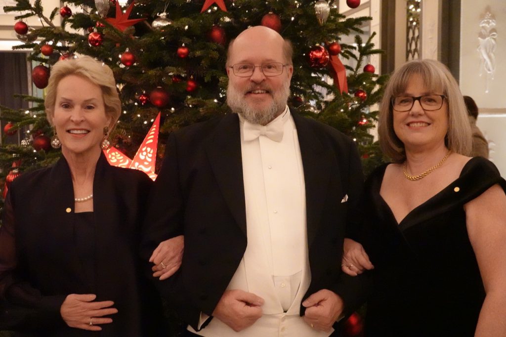
To Bill’s right is his sister, Frances Arnold, and to his left is Donna Strickland, former president of OSA who Bill got to know while he was president of SPIE. The occasion for the fancy attire? They are all in Stockholm last month at the Nobel Prize Award Ceremony, where Frances Arnold received the Nobel Prize in Chemistry, and Donna Strickland received the Nobel in Physics.
Smart definitely runs in the Arnold family.
How to Write a Good Scientific Paper
For the past 6 years, while serving as editor-in-chief of the Journal of Micro/Nanolithography, MEMS, and MOEMS, I have been researching and writing articles on how to write a good scientific paper. Recently I have turned that work into a book. It has been published by SPIE, who is generously making the electronic version of the book available for free in order to widen its distribution and impact. You can find a pdf of the book here, which you are free to use and distribute as you see fit. Information on the print version (which is for sale at a modest price) can be found here: https://spie.org/
This short (100 page) book is full of practical advice that anyone who wants to write a scientific paper (beginner or experienced writer) can use.