
(This post is certified ChatGPT-free.)
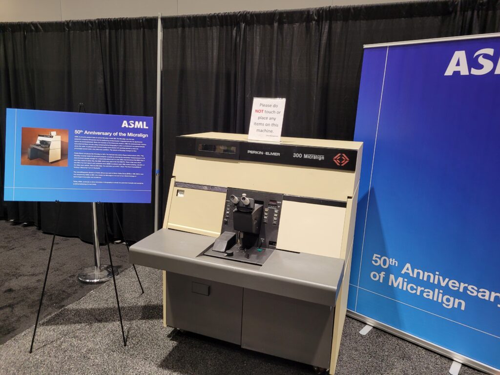
The day began with a second plenary, starting with ASML/SVGL/Perkin-Elmer veteran Chip Mason describing the history of the first commercial projection lithography tool, the Micralign, on the occasion of its 50th birthday. I am very sorry to say that another commitment prevented me from attending Chip’s talk, but numerous people (young and old) told me that it was fantastic. My first job as a lithographer (exactly 40 years ago this month!) involved supporting a fab with both a Micralign 300 and an Optimetrix 10X stepper, so the importance of the Micralign is also a bit personal for me. (Steppers were introduced five years later, in 1978, but the Micralign remained the workhorse of the industry well into the 1980s.) But not only did we hear about the Micralign, we get to see one. ASML now owns the former Perkin-Elmer site in Wilton, Connecticut where the Micralign was developed and manufactured, and they managed to find a Micralign in a garage somewhere (Vermont, I believe). The owner donated the tool and ASML had it shipped to San Jose where it is now on display (for one more day) in the Exhibitors’ Hall. Seeing a Micralign 300 in person is a wonderful opportunity.
Attending papers on Tuesday morning had me bouncing between sessions, as usual. Rudy Peeters of ASML gave an update on the readiness of high-NA EUV tools, including the status of the the four major components of the tool (source, reticle stage, wafer stage, and projection optics). Three EXE:5000 sources have been qualified (benefiting from commonality with sources from the low-NA tool), four wafer stages have been built (and are working towards testing at full acceleration), and one reticle module was built and is being tested. Multiple mirrors have been made, and so the next major milestone to watch for will be the first working projection optics box. It is fun to hear ASML express their optimism as if it were established fact: the goal of the high-NA EUV tool introduction in 2025 is to “replace EUV double patterning.” It is also interesting to infer the market ambiguity of this tool from statements like “high contrast imaging can be used for better images or better dose.”
Greg Denbeaux of SUNY Polytechnic (Albany) gave a very nice talk on attempts to move the idea of polymer aggregation as a source of resist stochastic variability from speculation to experimental measurement. By printing an open-frame EUV exposure at the dose to clear, residual resist at the substrate can be measured with an AFM to get some feeling of the size of the clumps of resist there. I wouldn’t call the method exactly quantitative, but it is a start.
Yaniv Abramovitz of AMAT looked at using in-device overlay measurement by a SEM at ADI (after develop inspect) rather than the traditional AEI (after etch inspect) measurements, and compared them to optical scribe-line measurements. His results from the classical skew experiment (where the scanner is directed to purposely offset the stage position of the second layer in increments, and then the measured overlay is plotted versus this scanner input skew) yielded unexpected slopes far less than 1. How could this be? Scanners have incredibly accurate stage positioning. AMAT has some more work to do.
Overlay and the role of stochastics in edge placement error (EPE) is my new special interest, so I spent the rest of the morning and much of the afternoon in sessions on those topics. Myungjun Lee of Samsung gave a fascinating talk on their development of hyper spectral imaging reflectometry for massive overlay and CD measurements. The traditional OCD (optical CD) approach collects reflected spectrum (reflectivity versus wavelength at a fixed angle) using a modest spot size (20 – 100 microns) aimed at a target of regular patterns (usually lines and spaces of fixed pitch). Analysis of the spectrum yields measurement of the CD, and possibly other information about the features. Spectral “imaging” reflectometry shrinks the spot size (to about 5 microns in this case) and uses that spot as one pixel in a larger “image” of many pixels. It is only an image in the sense that imaging optics are uses to collect data from each pixel in parallel, so that this technique is essentially massively parallel OCD. How massive? 3200 x 3200 pixels covering a 20.8 mm x 20.8 mm field. The massive data that can result from this tool opens up many interesting use cases. It is my understanding that Samsung is looking for an equipment partner to commercialize the technology.
Several authors (starting with myself the day before) described how EPE measurements are best used as an input to a calculation of yield (or number of good die). Inho Kwak of Samsung showed that using a prediction of number of good die (generically called a KPI = key process index, in the jargon of the fab) during advanced process control (APC) resulted in a 5% improvement of dies in spec. The control strategy first suggests an adjustment of the dose of the second layer, then calculates the overlay correctables to achieve lowest EPE (rather than individually trying to match CD with dose, then overlay with the correctables). Harm Dillen of ASML and Franz Zach of KLA proposed similar approaches.
In the SEM measurements session I especially like John Villarrubia’s talk on three new SEM-based fundamental research projects at NIST. John is the author of a standard Monte Carlo simulator for SEM behavior called JMONSEL, and these new projects aim to fill in some gaps and improve the accuracy of this simulator. The first experimental piece will compare a top-down SEM image at low voltage to a STEM (scanning transmission electron microscopy) image at high voltage for the same sample and in the same instrument. The second experiment measures secondary electron yield of materials, with the benefit that the materials are deposited and then measured without exposing the films to the atmosphere. The third project seeks to improve the models in JMONSEL using the data from the first two projects. This is a very worthwhile activity, and I commend John and NIST for taking a leadership role in these investigations.
The last talk I attended was also one for which I was a coauthor. Genevieve Kane of IBM gave her first SPIE presentation – congratulations on a nice job!
The Micralign Model 300 mentioned above was gifted by Bill Parker of Creative MicroSystems – thank you Bill!
From SPIE it began it’s journey back home to the factory in Wilton Ct. After a short stop for refurbishment by our friends at BetaSquared Lithography, we look forward to having the tool on display at ASML in Wilton, ready for the 100th anniversary 🙂