Category Archives: General

Items that do not fit in other categories

Vladimir Ukraintsev, 1955 – 2019

Vladimir Ukraintsev
Vladimir Ukraintsev

I’m sad to report that Vladimir Ukraintsev died last Saturday. He was 64. I knew Vladimir from his long involvement in the Metrology conference of SPIE’s Advanced Lithography Symposium. He was conference chair this year, but his illness kept him from attending.

I enjoyed his rigorous mind and kind demeanor. Here are the details from his SPIE profile:

Vladimir Ukraintsev has PhD in Solid State Physics. Before joining Qorvo, Inc. Vladimir founded Nanometrology International, Inc., directed Technical Marketing at Veeco Instruments and developed metrology solutions for 6 technologies at Texas Instruments. Vladimir published over 85 articles focusing on development of metrology and characterization solutions for industrial applications.

Solar Panels, Year 2

What a difference one year makes. 2017 was my first year with solar panels, and I was very proud that I generated 96% of the electricity I used for the year (including the charging of my electric car – driving on sunshine!). Last year was not as astonishing, though still good. I generated 81% of my total home electric consumption. What changed? Consumption was up 6% in 2018, due to a much hotter summer (in Texas, AC is the big electricity hog). But even bigger, generation was down 10% due to many more cloudy days. I suspect that these two results will be the extremes, and about 90% generated solar power will be about average. I’m still happy with that.

Smart runs in their family

In the middle of the picture below is Bill Arnold, a familiar face to many lithographers. He was head of lithography at AMD for many years, become the head of a technology development group (TDC) at ASML, as well as Chief Scientist (I think I have the title right) at ASML. He always gives some of the best talks at the SPIE Advanced Lithography conference, and is a senior editor at JM3. In the field of lithography, he is one of the smartest guys around.

Frances Arnold, Bill Arnold, and Donna Strickland

To Bill’s right is his sister, Frances Arnold, and to his left is Donna Strickland, former president of OSA who Bill got to know while he was president of SPIE. The occasion for the fancy attire? They are all in Stockholm last month at the Nobel Prize Award Ceremony, where Frances Arnold received the Nobel Prize in Chemistry, and Donna Strickland received the Nobel in Physics.

Smart definitely runs in the Arnold family.

How to Write a Good Scientific Paper

For the past 6 years, while serving as editor-in-chief of the Journal of Micro/Nanolithography, MEMS, and MOEMS, I have been researching and writing articles on how to write a good scientific paper.  Recently I have turned that work into a book.  It has been published by SPIE, who is generously making the electronic version of the book available for free in order to widen its distribution and impact. You can find a pdf of the book here, which you are free to use and distribute as you see fit.  Information on the print version (which is for sale at a modest price) can be found here:  https://spie.org/Publications/Book/2317706.

This short (100 page) book is full of practical advice that anyone who wants to write a scientific paper (beginner or experienced writer) can use.

Solar Panels after One Year

A little over one year ago I turned on my solar panels at my house.  Now that a full year of use has passed, I can assess their effectiveness.  My goal was to generate from solar 100% of the electricity I use.  I didn’t quite make it – I generated 96% of the electricity my house consumed.  But that included charging my electric car for the year, which means I was driving on sunshine.

If you are anything like me, you want to geek out on all the numbers.  So here they are.

The Panels

  • I have 30 panels, 320 W each, for a total capacity of 9.6 kW (LG320 NeON2 MonoX Plus panels)
  • Installed cost:  $28,000
  • Austin Energy Rebate:  $7,500
  • Federal tax credit: $6,100 (30 percent of the cost of the system)
  • Net cost:  $14,400

Energy Usage and Generation for Year One

  • Consumed:  13.59 MW-h
  • Generated: 12.75 MW-h
  • Net Consumption:  540 kW-h

Monthly generation and consumption at the Mack house in 2017

Electric Car Energy Consumption

  • Nissan Leaf Miles Driven:  ~8,000/year
  • Mileage:  3.3 miles/kW-h
  • Approximate energy consumption:  ~2,400 kW-h/year (about 18% of my total house consumption)

Live from Monterey

It has been eight years since I have been to Monterey to attend the Photomask Technology conference, commonly known as Bacus.  The name Bacus comes from the group, the Bay Area Chrome User’s Society, that originally sponsored the conference before merging with SPIE.  Fall in Monterey is a beautiful time to think about masks!  And this year we have the added benefit of thinking about Extreme Ultraviolet Lithography (EUVL) as well.  The EUVL Symposium has also decided cooperated with SPIE to host their conference and this year the two meetings have been collocated for the first time.  The result is a great synergy that makes both conferences better and gave me the necessary excuse to come again.

The synergy seems to have worked, with 560 technical attendees and about 100 more attending just the equipment exhibit (significantly more people than the organizers had expected).  I missed most of the first day of the photomask conference, but managed to notice how trendy the topic of machine learning has become.  Unfortunately, this human didn’t learn enough to make much sense of the machine learning papers.

By Tuesday the EUVL conference had begun and I greatly enjoyed Greg McIntyre’s keynote talk on EUV readiness for manufacturing.  He pointed out how lithography scaling is slowing significantly, but that “device cleverness” is taking up the slack.  These one-time innovations (like reducing the number of wire tracks making up the height of a standard cell) are helping to keep density scaling on track.  The hope, then, is that EUV will arrive and get lithography pitch scaling back up to speed.  Greg also clearly identified stochastic yield loss (extremes of roughness) as the number one problem facing EUV lithography.  When printing lines and spaces (or contact holes) is there a process window that enables no bridges and no breaks (no “missing or kissing” contact holes) at the same time?  Some significant metrology innovations may be needed to answer this question.

Many speakers discussed the imminent availability of the 250W EUV light source from ASML.  Word on the street (or at least the conference halls) says Samsung is getting this first 250W source on their first NXE:3400B scanner.  It has already shipped is supposed by be up by the end of this year with first results in early 2018.  Everyone will be waiting anxiously for those results, I am sure.

It is now clear that ASML is positioning the 3400 as the first EUV high-volume manufacturing (HVM) scanner.  It looks like most of the NXE:3300 and 3350 tools will not be upgraded to higher source powers (many will stay at 80W) and will remain learning tools.  The transition to a high power source is not an easy one.

Besides the ability to handle higher source powers, the 3400 has other improvements, most particularly the ability to use extreme off-axis illumination (out to sigma of 1) with half the pupil fill ratio (20%) of previous generation tools.  This will allow k1 as low as 0.32 (down from 0.38 or so).  Zeiss has shipped 12 of the 3400 optical systems to ASML to date.

Progress on EUV lithography as reported at the conference continues to be good, but none of the major risk factors have yet to be retired:  sufficiently high source power to achieve good throughput, making and maintaining defect-free masks, and no yield loss due to stochastic effects in lithography.

Erik Hendrickx of imec gave an update on their efforts to identify new absorber materials for EUV masks.  The current tantalum absorber requires a thickness of 55nm, resulting in tall structures with undesirable shadowing effects for tilted illumination.  Absorbers like Nickle or Cobalt could shrink the thickness below 35nm.  The problem is etching these materials, and more work is still required.

Heebom Kim of Samsung was optimistic about making defect-free masks.  They have developed their own internal actinic mask inspection system that seems to have put Samsung ahead in EUV mask making.  He claimed a current mask yield of 90%.  They will also be getting the first EUV AIMS tool from Zeiss next year in order to qualify repairs with actinic light.  But the combination of expensive inspection plus expensive repair verification plus expensive blanks will make EUV masks cost 8 times more than a 193 mask.  Wow.  I remember 15 years ago hearing promoters of EUVL saying that one of the big benefits of EUV will be cheaper masks compared to 193.  Whenever I feel a need for a good laugh, I go back and look at those early cost projects (when an EUV scanner was going to cost $20M, for example).

The resist papers focused on understanding the exposure mechanisms of EUV resists, and on reducing roughness.  Bits of progress were made on both fronts, but not nearly enough to reduce the risk of stochastic problems delaying or stopping the use of EUV in manufacturing.  I’m not sure what a major breakthrough in roughness management will look like, but it won’t look like what we saw this week.

ASML’s one billion euro investment in Zeiss is showing tangible effects as construction has begun on new buildings for the manufacture of high-NA EUV optics.  The NA=0.55 tool will be bigger than a freight train locomotive, and is essentially a two-story building.  If you thought $140M was a lot for an NA=0.33 EUV scanner, imagine how expensive the new NA=0.55 tool will be.  Then imagine higher.

On Thursday I skipped over to the photomask conference to hear about progress on multibeam tools for mask making.  Both IMS and NuFlare are making 50KeV e-beam lithography tools with 512X512 beams.  IMS has hit the market first and has already shipped many tools targeting the N7 node.  NuFlare has a beta version of their tool installed at Samsung, and so is behind IMS.  Their tool is spec’d for a higher resolution, however, and is geared toward the N5 node.  The competition is encouraging and both companies are making great progress, enabling future mask making with improved specs and reasonable write times.

Vinayan Menon of imec gave an extremely refreshing talk – an unfiltered look at one year in the life of an EUV scanner.  It wasn’t pretty.  After installing an ~80W source on their 3300, imec faced a series of ugly trade-offs:  either operate the source at near its full power and live with extremely low tool availability, or operate at a much lower power (below 30W) in order to keep the tool running and available.  There was also a fairly significant reduction in source power over time that shows rate is not equal to actual power.  Tool upgrades could help things, but those upgrades often took one or more months, so imec chose availability over peak performance.  I found another point he made intriguing as well.  A focus difference between the two chucks of the scanner was first detected as a systematic difference in linewidth roughness, suggesting that LWR might be a good focus monitor.

The closing remarks of the EUVL Symposium always include the results of a survey of the conference steering committee.  The basic survey asks which potential roadblock for EUV success is most concerning.  This year’s survey asked two questions:  what is most concerning for initial HVM insertion, and what is most concerning for continued advances in EUV lithography beyond initial insertion.  Interestingly, while the availability of a high-power source was considered the most pressing issue for initial HVM insertion, stochastic-induced variation was considered the number one issue for continued advances in EUV lithography.

Unfortunately I missed quite a few good papers at the conference.  I was busy rehearsing.  For many of the EUV crowd new to the Bacus confer
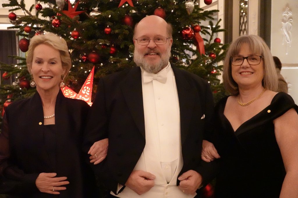
ence, it was a surprise to discover that the conference banquet on Wednesday night was followed by an entertainment show put on by members of our community (three of the six cast members had papers at the conference).  This 40 minute show is skit humor, replete with singing, dancing, and often a fair amount of silliness (if you can’t imagine what I’d look like in an elf costume, don’t try).  I was very glad to be a part of the show this year after a 12-year hiatus.  I hope the audience had half as much fun watching it as we did putting it on.  (Photo Credit:  Bernd Geh)

SPIE Advanced Lithography Symposium 2017 – day 2

I write my posts the morning after that day of the symposium. And today definitely feels like a “morning after”.  Two days of late nights at the hospitality suits followed by far too little sleep are beginning to have their effects.  Let’s see if adrenaline and desire can carry me through the rest of the week…

For those reading this blog who do not attend the SPIE Advanced Lithography Symposium, let me explain that there are seven conferences as a part of the symposium, and there are always at least five sessions happening in parallel (Wednesday morning will see all seven).  There is almost always more than one paper at any given time that I want to see, but all of my attempts at quantum entanglement with a doppelgänger have led to decoherence.  (Yes, that is the ultimate in bad nerd humor.)  Be aware that my extremely limited sampling of the symposium does not begin to do it justice.

For me, the day started with ASML’s talk on their new NXE:3400 EUV scanner, soon to be released.  As a bit of history, the NXE platform was introduced to us at this symposium in 2010.  The NXE:3100 was a “pre-production” tool, described in this way:  “With an NA of 0.25 and a productivity of 60wph this tool is targeted for EUV process implementation and early volume production at the 27nm node.”  But the NXE:3300 was to be the true production tool, targeted at 125 wph and the 22nm node.  As we all know, the 3300 missed its window for use in production, but the much improved NXE:3350 soon become the target production tool.  Since there was an upgrade path from the NXE:3300 to the NXE:3350, there was still a chance for those first 3300s to be used in production.  But after listening to Intel’s Monday talk, I am getting the impression that all the existing tools in the field are playing the original role of the original 3100.  It is the NXE:3400 that is now the targeted tool for high volume manufacturing.  It has many improvements (such as the Flex-illuminator and a membrane just above the wafer that blocks unwanted out-of-band radiation), with throughput again targeted at 125 wph.

A quick word about throughput.  Since throughput is a function of the dose used to expose the resist, and this dose is decided by the customer, ASML must make some assumption about the dose in order to specify the throughput of their tool.  In the very early days of EUV development (15 years ago), many people hoped for a 5 mJ/cm2 sizing dose.  That dream quickly relaxed to the more realistic (but still unrealistic) 10 mJ/cm2.  The throughput specs for the NXE:3100 were based on this assumed dose.  But since pattern quality improves with higher dose, the production spec of 125 wph for the NXE:3300 was based on a dose of 15 mJ/cm2.  Since then, the unforgiving onslaught of stochastic randomness brought a concession by ASML to a dose of 20 mJ/cm2.  This is now the assumption used to predict a 125 wph throughput for the NXE:3400.  This dose is also a function of the mask level being printed, with contact holes, vias, and cut masks requiring more dose (maybe twice as much, possibly more).  Since I don’t think that a dose of 20 mJ/cm2 is remotely possible due to roughness effects, significant downward scaling of the true throughput from the specified value is inevitable.

I enjoyed Tim Brunner’s paper on how to intelligently determine roughness specifications (but as a co-author, I am certainly biased).  The old ITRS specifications for linewidth roughness, useful in their day, and now rightly ignored as both irrelevant and unachievable.  Tim’s results, though, are scary.

I know that I exhibit selection bias, since I seek out the papers that deal with roughness and stochastic effects, but is seems that stochastics are everywhere at the symposium this year.  From linewidth control specifications to edge placement error, stochastic effects are almost never ignored anymore and often are admitted to be the dominant source of error in the lithography process.  After years of complaining that roughness was not getting the attention it deserved, that no longer seems to be a problem.

At the resist conference (Advances in Patterning Materials), the theme was often better roughness through chemistry.  Or if we don’t have the chemistry ready, it is often better roughness through cartoons of the chemistry.  Let me explain a test that I use when examining proposed solutions to stochastic-induced roughness:  If I don’t understand how it works, I don’t believe it.  Granted, this convolves skepticism with my own quite considerable ignorance, so I have to continually try to find my own errors in thinking and be open to being convinced.  Some ideas that fall into the “don’t understand, so don’t believe” category include PSCAR and second-order deprotection kinetics.  I hope to be convinced (preferably with good LER data).

We are half way through the technical conferences.  I have two more papers to give, and many more to listen to.

SPIE Advanced Lithography Symposium 2017 – day 1

The first day of the symposium began with the awards.  I was very happy to see a great group of new SPIE fellows from our community:  Emily Gallagher of Imec, Yuri Granik of Mentor Graphics, Qinghuang Lin of IMB, David Pan of the University of Texas at Austin, Mark Phillips of Intel, and James Thackeray of Dow.  Congratulations to each of you for this well-deserved recognition.  Donis Flagello, CEO of Nikon Research Corporation of America, won this year’s Frits Zernike award (full disclosure, I nominated him).  For a history of the Zernike award, see this brief article.

For a change, I enjoyed all three plenary speakers.  Usually, at least one is a dud, but not this year.  I have to admit that I didn’t care for JSR CEO Nobu Koshiba’s disciple-like references to Ray Kurzweil and his singularity predictions (I’m not a Kurzweil fan), but it was just one part of his overall optimism for Moore’s Law.  I don’t agree that Moore’s Law will continue to the 2-nm node, but I guess it’s important that sufficient optimism exists, otherwise we’ll never try.  And we should try.

The first two talks of the EUV session were keynote addresses.  Britt Turkot of Intel painted a fairly rosy picture of the progress of EUVL towards manufacturing readiness.  “It’s been a long and winding road,” and we still have a ways to go, but the eight NXE:3300s and six NXE:3350s in the field are giving semiconductor manufacturers opportunities to shake out enough of the reliability problems to enable process learning.  Tool availability continues to creep up (past the 70% mark), and mask making has progressed to the point where Intel has made “multiple” defect-free EUV masks.  Intel showed data on “adders” (defects that get added to the mask during use) and reiterated their message from last year that that production without a pellicle is not an option.  Thus, it makes sense that she listed the availability of a manufacturing-capable pellicle as the biggest risk.

She also mentioned stochastics, saying that “CD and edge placement variability is a deal breaker.”  But then her conclusion slide said that resist performance won’t gate the introduction of EUV.  I didn’t know what to make of these mixed messages, especially when she explained that the target dose for EUV manufacturing was 20 mJ/cm2.   At that dose, there will be plenty of CD and edge placement variability.

Seong-Sue Kim of Samsung was similarly encouraged by EUVL improvement.  He expressed amazement at the progress in mask blank defectivity saying it had reached the benchmark of 5 defects per blank that he thinks can enable manufacturing.  He also said that the mask blistering problems he mentioned last year have largely been solved.  For resists, he thinks that current performance is good enough for 7nm development, but sensitivity (at low roughness) needs to be improved for production.  Of course, everyone agrees with that statement.  The question is how to do it.

My favorite technical talk was Bill Hinsberg’s modeling of metal-oxide resists – a much needed start.  John Biafore gave a great paper modeling millions of contact holes at various EUV conditions and looking for stochastic-related failures.  He expressed skepticism at any possible breaking of the RLS trade-off (“resolution, LER, sensitivity – pick two”).

Finally, I was extremely gratified by the reception I received to my tutorial talk and was grateful for the many people willing to stay till 6:30pm to hear me speak.  Thanks to Eric Panning and Ken Goldberg and the EUV Lithography conference for giving me such a great opportunity to talk about stochastic-induced roughness.

SPIE Advanced Lithography Symposium 2017 – a prologue

The week before the annual SPIE Advanced Lithography Symposium is always a busy one for me, but this year it is particularly so.  It’s not just because I am giving a short course and three conference presentations.  And it’s not because I am coauthor on four other talks (that’s a total of seven papers – yikes!).  No, the real reason I am way too busy this week is that yesterday I launched my new company – Fractilia.

Seventeen years ago I sold my lithography simulation company FINLE Technologies, and after five years at KLA-Tencor I settled into the life of the “Gentleman Scientist”.  My goal was to contribute to the science and practice of lithography through my research, teaching, and writing, all the while looking into the problems that I thought were the most interesting.  For the last 10 years that “most interesting problem” has been stochastic-induced roughness.  It is an incredibly interesting, fun, and important topic, and I have written 25 papers since 2009 that I hope have contributed something to our community’s understanding of this vexing problem.  My goal has been to help transform our understanding of stochastics and roughness, so that we can better tackle the problem of reducing it.

Recently, though, I’ve come to understand that the best way for me to realize my vision of making a positive impact on the industry is to commercialize my ideas in software.  So I’ve teamed up with my old partner from the FINLE days, Ed Charrier, to start a new company (Fractilia) and to introduce a new product (MetroLER).

The goal of Fractilia is to bring rigor, accuracy, and ease-of-use to the analysis of stochastic-induced roughness in semiconductor manufacturing and process development.  Fractilia will deliver something I think is currently lacking in the industry:  accurate and repeatable analysis of SEM images to extract the true, unbiased roughness behavior of wafer features.  I think the industry needs this product.  Of course, the market will tell me if I am right.

So, as I have for the last several years, I’ll be giving papers next week on various ways in which the measurement of pattern roughness can go wrong.  I’ll complain about errors in the SEM and how they hide the true roughness behavior on the wafer.  I’ll moan about the statistical difficulties of sampling, aliasing, and biases in our measurements.  But this year I’ll do more than complain – I’ll do something about it.

For the interested reader, here is a recent press article on the new company:

http://semiengineering.com/fractilia-pattern-roughness-metrology/

And here is the company website:  www.fractilia.com

Now, it is back to writing papers.  See you in San Jose!