Tag Archives: SPIE

SPIE Advanced Lithography and Patterning Symposium 2023 – day 4

I began the last day of the conference at the EUV talks.  Jo Finders of ASML described how non-idealities of the scanner can effect single-layer edge placement errors (a combination of CD errors, both global and local, and local pattern placement errors).  This was the first time I had seen a numerical breakdown of mechanisms of “NILS loss”, the reduction of the Normalized Image Log-Slope from its theoretical value caused by mask topography, aberrations, flare, focus variation across the slit, etc.  The NILS loss totaled to 15%, and Jo described various approaches to get some of that back.

Suk-Koo Hong of Samsung provided “speculations” on why pushing k1 below 0.4 in EUV is problematic (specifically, for printing contact holes).  The reason is stochastics, and there seems to be a scaling with pitch and CD that is worse than the famous z-factor predicts:  z-factor = feature size^3 * LCDU^2 * Dose-to-size.  Plotting LCDU (local CD uniformity) versus dose produces higher than expected LCDU at the lowest doses and seems to be following a different iso-z-factor limit.  The specifics of CD and pitch and anything else that made up the data points in his graphs, however, were not revealed.  Still, it was an interesting way to look at the problem, one still without a solution.

As an aside, Samsung gave many papers this week, and some of those papers were some of the best in the conference.  Case in point: Hyungju Ryu presented work by Sangjim Kim (who couldn’t make it here) on process control for EUV metal oxide resists (MOR, read Inpria).  The two MOR challenges are CD variation due to sensitivity to humidity, and poor etch resistance.  Apparently, these problems are well known to the users of Inpria resists, but they weren’t being discussed publicly until now.  For example, CD was shown to vary by 2 – 8% depending on the post-coating delay.  Samsung showed, however, that careful optimization of every resist processing step reduced the CD variation to 35% of its original value.  Etch resistance of the MOR was not as good as expected since partially exposed resist does not have a well-connected network of core-to-core bonds necessary for best etch resistance.  Samsung’s solution was a UV flood exposure.  They said that more work was required to make the MOR ready for high volume manufacturing, but these were good steps in that direction.

On a completely different topic, Etienne Poortere of ASML showed how a carefully designed test mask coupled with voltage contrast metrology could be used to establish design rules for via connections to metal 1 in a dual damascene process of 28 nm pitch.  The technique made evaluation of a matrix of tip-to-tip spacings and M1 via overlap rules quite easy.

Back in the SEM world, Ofer Adan gave a good marketing talk on Applied Materials’ new cold field emission (CFE) electron source for their inspection SEMs (and maybe for the CD SEM?  It wasn’t clear.).  I’m convinced this new CFE source is better, but I don’t know why.

As is usually the case, by Thursday afternoon my brain had reached its absorption limit.  I continued going to talks, but my notes became brief as my attention strayed.  Summing up, this week lived up to my expectations – it was the Advanced Lithography and Patterning conference back to its full glory.  There were many solid talks – nothing earth shattering (but there rarely is), just good incremental progress towards the harder to reach goal of keeping Moore’s Law alive.  It’s a shame that the memory sector downturn kept many Micron and SK Hynix lithographers away, and that Intel’s troubles kept their attendance to a minimum.  It was gratifying to see so many good papers from Samsung, and decent attendance from TSMC.  I go away looking forward to next year.

SPIE Advanced Lithography and Patterning Symposium 2023 – day 3

Bright and early, the talks begin at 8:00 am.  From Mark van de Kerkhof of ASML, and then Joost Bekart of imec, we got two updates on EUV pellicles.  The composite (metal-silicide) pellicles are the second-generation pellicle after polysilicon, but they are stalling out with transmission near 90%.  Higher transmission requires thinner pellicles, which is quite difficult.  The low transmission also limits the highest power that can be used (absorption heats up the pellicle, and if the heat cannot be removed fast enough the temperature rise will ultimately destroy it).  Slow progress can be expected, but it seems that increases in source power will outpace increases in transmission.  That is why the carbon nanotube (CNT) pellicle, first proposed by imec in 2015, is so interesting.  It has extremely high transmission (> 97% after being annealed to remove contaminants) and so can withstand very high source power (> 1000W).  It’s drawback is the gradual thinning of the pellicle with use as the carbon (activated by all the EUV light) reacts with hydrogen gas, which ASML puts in the system specifically to remove carbon deposits that might occur inside the tool!  An interesting dilemma, and I will enjoy watching progress towards a solution.

Back in the metrology session Yoshihiko Fujimori of Nikon introduced a new tool for high-density CD measurements on the wafer.  The paper was sparse on some important details, but the tool reminded me of a crystallography setup, measuring the diffraction pattern of the whole patterned wafer with variable wafer and detector angles.  (The name AMI-5700, along with a marketing picture, indicated at least close to commercial readiness.)  A full wafer, up to 100,000 points, can be measured in a couple of minutes.  That means about a 1 mm spatial resolution, and it is obviously limited to periodic structures (and so memory chips).  The key idea appears to be correlating various “signals” coming from the detected diffraction pattern with SEM-based measurements of CD in a previous calibration step.  Then a measurement of that signal across the wafer is used to infer CD variation across the wafer.  Like all such techniques, the two key questions are sensitivity to noise, and sensitivity to other systematic variations (such as an underlying film thickness) that might also impact the signal being monitored.  These problems have bedeviled other similar attempts in the past.

Gian Lorusso of imec gave a fast-paced overview of the metrology of thin versions of the dry Lam Research resist.  As Gian has shown in the past, low signal-to-noise ratio CD-SEM images that often result from very thin resist patterns can make accurate metrology difficult (even when using state-of-the art metrology software from Fractilia!).  The main message from this paper is the happy fact that the Lam dry resist offers fairly high material contrast in the SEM, making measurement of even 10 nm thick resist patterns acceptable at normal SEM settings (such as 16 frames of averaging).

On the topic of resist shrinkage in the CD-SEM (a problem that never goes away, no matter how much we ignore it), Musaki Sugie of Hitachi offered an interesting combination of ideas.  As many SEM vendors have demonstrated, going to 100 V reduces shrinkage, though it increases the noise in the image.  (Ran Alkoken of AMAT showed their 100 V CD-SEM in the following talk.)  This voltage was coupled with an optimized scan speed to minimize charging and to prevent CD measurement repeatability from suffering.  An interesting additional idea in the talk was to average together 32 sub-sections from a large 1-frame image of lines and spaces to measure CD with the precision of a 32-frame image and the shrinkage of a 1-frame image.  Information such as linewidth roughness or local CDU cannot be obtained, but for the one goal of finding the CD with minimal shrinkage, the approach may work.  As an aside, he noted that metal oxide resist (that is, Inpria) has 3X less shrinkage than chemically amplified resists for EUV.

After lunch I saw a few papers from imec, updating prior efforts.  Andreas Frommhold used Mark Maslow’s concept of Tail CD (measured mean +/- 3sigma of the contact hole distribution) as a predictor of merged contact hole rates.  In this case, the CD being measured was the gap between the holes, and the mean – 3sigma value is correlated with rates of merged holes.  I know from experience, however, that exactly how one defines and measures this hole-to-hole gap CD is quite critical.  Lieve Van Look of imec continued her very detailed work on local MEEF (mask error enhancement factor) and its impact on LCDU, bringing the concept of MEEF into the era of stochastics.  Her collection of papers on this topic so far represents the definitive work on the topic.

The poster session in the evening was, thank goodness, in a massive hall with plenty of room to work your way among the posters without being jammed in by the crowds (which frequently happens at other conferences).  Alas, being a long-time participant in this conference meant that my mean free path (the average distance traveled before running into someone to talk to) was very small.  I didn’t see many posters.  For all the poster presenters out there – please turn in a manuscript of your paper so I can read them!

SPIE Advanced Lithography and Patterning Symposium 2023 – day 2

(This post is certified ChatGPT-free.)

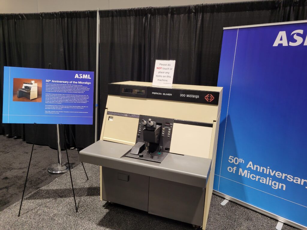
The day began with a second plenary, starting with ASML/SVGL/Perkin-Elmer veteran Chip Mason describing the history of the first commercial projection lithography tool, the Micralign, on the occasion of its 50th birthday.  I am very sorry to say that another commitment prevented me from attending Chip’s talk, but numerous people (young and old) told me that it was fantastic.  My first job as a lithographer (exactly 40 years ago this month!) involved supporting a fab with both a Micralign 300 and an Optimetrix 10X stepper, so the importance of the Micralign is also a bit personal for me.  (Steppers were introduced five years later, in 1978, but the Micralign remained the workhorse of the industry well into the 1980s.)  But not only did we hear about the Micralign, we get to see one.  ASML now owns the former Perkin-Elmer site in Wilton, Connecticut where the Micralign was developed and manufactured, and they managed to find a Micralign in a garage somewhere (Vermont, I believe).  The owner donated the tool and ASML had it shipped to San Jose where it is now on display (for one more day) in the Exhibitors’ Hall.  Seeing a Micralign 300 in person is a wonderful opportunity.

Micralign 300 by Perkin-Elmer
Micralign 300 by Perkin-Elmer on display at the SPIE Advanced Lithography and Patterning Symposium

Attending papers on Tuesday morning had me bouncing between sessions, as usual.  Rudy Peeters of ASML gave an update on the readiness of high-NA EUV tools, including the status of the the four major components of the tool (source, reticle stage, wafer stage, and projection optics).  Three EXE:5000 sources have been qualified (benefiting from commonality with sources from the low-NA tool), four wafer stages have been built (and are working towards testing at full acceleration), and one reticle module was built and is being tested.  Multiple mirrors have been made, and so the next major milestone to watch for will be the first working projection optics box.  It is fun to hear ASML express their optimism as if it were established fact:  the goal of the high-NA EUV tool introduction in 2025 is to “replace EUV double patterning.”  It is also interesting to infer the market ambiguity of this tool from statements like “high contrast imaging can be used for better images or better dose.”

Greg Denbeaux of SUNY Polytechnic (Albany) gave a very nice talk on attempts to move the idea of polymer aggregation as a source of resist stochastic variability from speculation to experimental measurement.  By printing an open-frame EUV exposure at the dose to clear, residual resist at the substrate can be measured with an AFM to get some feeling of the size of the clumps of resist there.  I wouldn’t call the method exactly quantitative, but it is a start.

Yaniv Abramovitz of AMAT looked at using in-device overlay measurement by a SEM at ADI (after develop inspect) rather than the traditional AEI (after etch inspect) measurements, and compared them to optical scribe-line measurements.  His results from the classical skew experiment (where the scanner is directed to purposely offset the stage position of the second layer in increments, and then the measured overlay is plotted versus this scanner input skew) yielded unexpected slopes far less than 1.  How could this be?  Scanners have incredibly accurate stage positioning.  AMAT has some more work to do.

Overlay and the role of stochastics in edge placement error (EPE) is my new special interest, so I spent the rest of the morning and much of the afternoon in sessions on those topics.  Myungjun Lee of Samsung gave a fascinating talk on their development of hyper spectral imaging reflectometry for massive overlay and CD measurements.  The traditional OCD (optical CD) approach collects reflected spectrum (reflectivity versus wavelength at a fixed angle) using a modest spot size (20 – 100 microns) aimed at a target of regular patterns (usually lines and spaces of fixed pitch).  Analysis of the spectrum yields measurement of the CD, and possibly other information about the features.  Spectral “imaging” reflectometry shrinks the spot size (to about 5 microns in this case) and uses that spot as one pixel in a larger “image” of many pixels.  It is only an image in the sense that imaging optics are uses to collect data from each pixel in parallel, so that this technique is essentially massively parallel OCD.  How massive?  3200 x 3200 pixels covering a 20.8 mm x 20.8 mm field.  The massive data that can result from this tool opens up many interesting use cases.  It is my understanding that Samsung is looking for an equipment partner to commercialize the technology.

Several authors (starting with myself the day before) described how EPE measurements are best used as an input to a calculation of yield (or number of good die).  Inho Kwak of Samsung showed that using a prediction of number of good die (generically called a KPI = key process index, in the jargon of the fab) during advanced process control (APC) resulted in a 5% improvement of dies in spec.  The control strategy first suggests an adjustment of the dose of the second layer, then calculates the overlay correctables to achieve lowest EPE (rather than individually trying to match CD with dose, then overlay with the correctables).  Harm Dillen of ASML and Franz Zach of KLA proposed similar approaches.

In the SEM measurements session I especially like John Villarrubia’s talk on three new SEM-based fundamental research projects at NIST.  John is the author of a standard Monte Carlo simulator for SEM behavior called JMONSEL, and these new projects aim to fill in some gaps and improve the accuracy of this simulator.  The first experimental piece will compare a top-down SEM image at low voltage to a STEM (scanning transmission electron microscopy) image at high voltage for the same sample and in the same instrument.  The second experiment measures secondary electron yield of materials, with the benefit that the materials are deposited and then measured without exposing the films to the atmosphere.  The third project seeks to improve the models in JMONSEL using the data from the first two projects.  This is a very worthwhile activity, and I commend John and NIST for taking a leadership role in these investigations.

The last talk I attended was also one for which I was a coauthor.  Genevieve Kane of IBM gave her first SPIE presentation – congratulations on a nice job!

SPIE Advanced Lithography and Patterning Symposium 2023 – day 1

The plenary session Monday morning began with awards.  I was glad to hear that 27 students received grants from SPIE to cover their registration and travel to the conference (Fractilia is one of the corporate sponsors of these student grants and I was happy to meet some of those students later that day at a student-mentor lunch).  Tony Yen of ASML was this year’s winner of the Frits Zernike Award for Microlithography – congratulations!  The Kingslake Award for Optical Design is not usually presented at this conference, but this year’s winner Wilhelm Ulrich chose to receive that honor here since his work at Zeiss in designing lithographic lenses was the reason for this prestigious reward.

Was saw eight new SPIE fellows from our community inducted this year, seven of whom were on hand to be recognized for this achievement: Martin Burkhardt of IBM, Debbie Gustafson of Energetiq, Larry Melvin of Synopsis, Warren Montgomery of EMD Electronics, Linyong Pang of D2S, Takashi Sato of KIOXIA, Geert Vandenberghe of imec, and Yayi Wei of the Chinese Institute of Microelectronics.  A great group of fellows, indeed.

As I glanced back across the room before the start of the first plenary talk, I was gratified to see what once was a familiar site:  the largest lecture hall at the San Jose convention center was full to overcrowding, standing room only, with an overflow room set up to accommodate the rest.  We are back!  And our first plenary speaker of the day, Martin van den Brink of ASML, did not disappoint in a talk densely packed with interesting information.  Martin gave a plenary speech 15 years earlier where he projected scaling for the coming 15 years, so it was fun to hear him compare those projections to reality (he did better than most prognosticators) and then try it again, providing ASML’s vision of Moore’s Law in the coming decade.  Of course, he predicted lithography scaling would continue – it is in ASML’s DNA (and I suspect in their corporate bylaws as well).

Martin described the well-known evolution of Moore’s Law away from transistor scaling towards system scaling, especially for energy efficient performance (EEP).  Still, he remains hopeful that DRAM scaling will continue down to 15 nm pitch, and vertical NAND flash will grow to 1000 transistors tall!  ASML is pushing massive e-beam inspection to approach optical defect inspection in terms of productivity, a tough road, but I am sure they will be at least partially successful.  I was almost numbed to see projections of DUV scanner throughput to 400 wafers per hour, and even 500 wph!  My first thought was “that’s impossible”, but I’ve come to understand that these kinds of things are impossible only until ASML does them.  Of course sustainability is on everyone’s mind nowadays, so Martin addressed the 100 kW-hour per finished wafer energy expenditure for lithography.  The goal is for that number to at least remain the same, if not go down over time.  As for EUV source power, 500W is said to be on the way, 600W is being demonstrated, and 800W is on the roadmap.  Each increase is EUV source power is of course very challenging.

Maybe the most interesting part of his talk (at least for me) was the new optical designs that removed one mirror from both the 0.33 and 0.55 NA systems (from the illuminator, it appeared).  Since each mirror has less than 70% reflectivity, the removal of one mirror represents a significant throughput advantage for these EUV scanners. He also described ASML’s plans for EUV “hyper” NA, a 0.75 NA design.  But without polarization (which Martin admitted would not happen), the image contrast benefit of the higher NA is reduced, so that a cost/benefit analysis of hyper-NA EUV seems clearly against it ever becoming a reality.  Time will tell, but of course ASML must have a roadmap.

I did not stick around for the second plenary talk on the Chips Act (I’m not going to apply for any of that money), so it was off to the regular conference papers.  Martin Weiss of Intel talked about modeling the matching of high-NA EUV two-field to low-NA one field difficulties.  It seems Intel is still hoping to jump back into the lead in scaling by being the first to implement high-NA EUV into production.  Good luck to them – that is going to be very hard, and probably late.  Zhigang Wang and B.H. Lee of Hitachi High Technology talked on the future of CD-SEM metrology, emphasizing the need for 0.01 nm tool-to-tool matching (or at least of that order) without giving much of a hint how they might achieve that.  I agree with them that SEM tool matching needs significantly more attention.  Ryosuke Kizu of the National Metrology Institute of Japan gave another good paper this year on their metrological tilt-AFM tool.  This year they looked at how SEM exposure of resist results in sidewall roughness smoothing – an important topic for those of us trying to measure resist feature roughness using top-down CD-SEMs.  I hope Kizu can partner with a CD-SEM owner to turn this interesting experimental technique into results useful to semiconductor metrologists.

In the EUV+Optical/Resist joint session in the afternoon there were a pair of papers by FujiFILM followed by Samsung looking at developer and rinse effects on line-edge roughness.  Both seemed to indicate that NTD (negative tone develop) using solvent developer for EUV held some promise for roughness and defect reduction, but I would consider these results preliminary at best.  I hope they work with imec to validate this behavior.

While there were a few other good papers late in the afternoon, my business obligations prevented me from attending them.  I had to go to the Fractilia Happy Hour at Uproar Brewing.  Ah, the burdens of entrepreneurship.

SPIE Advanced Lithography and Patterning Symposium 2023 – day 0

It looks like we are back to normal.  After three years where Covid 19 was on everyone’s minds and tongues (if not yet in the upper respiratory tracts), today more people seem interested in snow on the mountains surrounding San Jose, the massive downtown in the memory business, the nasty weather outside, and who survived the layoffs at company xyz.  Different is the new normal.  It is good to be back!

The conference itself is back to its former vigor.  Compared to 2019, submissions are up (over 450), attendance is about the same (over 2000 seems likely), and the number of exhibitors is about the same (a low 54).  I had 11 people in my all-day short course on Sunday (lower than hoped, but a great group!).  And the reconnecting with friends has already begun. From a technology perspective, what will the week be like?  I have to admit that I am completely clueless.  I haven’t yet dived into the agenda of talks (I miss the printed programs), and only know that I need to be at the plenary program at 8am on Monday.  My one talk is Monday at 2:30pm, and the Fractilia Happy Hour is also Monday, so that day is my current focus (I’ll think about Tuesday on Tuesday).  And so another week at ALP begins…

SPIE Advanced Lithography and Patterning Symposium 2022 – day 4

The mood at the conference this week can be summed up in one word:  happy.  We were all just happy to be here, with smiles visible everywhere, even under masks.

Thursday morning began with a quite philosophical keynote talk in the metrology session on the role of MI (metrology and inspection) in semiconductor manufacturing by Younghoon Sohn of Samsung.  He touched on broad subjects like the role of sampling (depends on the failure rate), the dilemma between resolution and speed in inspection (and the wide gulf in both between optical and e-beam inspection), and the basic roles of MI (define a process window, identify cause and effect, and process monitoring and control).

A joint session between Optical/EUV and Etch provided several nice papers.  Angelique Raley gave an overview of three techniques being promoted by TEL:  a spin-on SiC underlayer for EUV to prevent pattern collapse, a development process (not really explained) called ESPERT for Inpria resists that also prevents pattern collapse by improving the sidewall profile, and a cryogenic etch for lower LCDU (local critical dimension uniformity) and defectivity.  Roberto Fallica of imec gave a quote that I like (and often say myself), “Stochastics is the major roadblock for EUV Lithography”.  He then talked about a “healing” etch process that reduces contact hole LCDU through an aspect ratio dependent etch rate (high aspect ratio resist patterns etch faster, causing narrow holes to widen, while low aspect ratio resist patterns etch mode slowly, causing wide holes to narrow).  One interesting (and confusing) result was that the dose that provided smallest LCDU was not the dose that gave the lowest defectivity.  Finally, Qinghuang Lin of Lam talked about the application of Lam’s new dry-deposited and dry-developed resist to contact holes (I was not able to catch Rich Wise’s earlier paper on its application to lines and spaces).

Since I left after lunch to catch a plane home, I was not able to see what I’m sure were some good papers on the last afternoon of the symposium.  After a valuable and rewarding week here in San Jose, I was still anxious to get home.  Looking back two years, here is how I ended my Advanced Lithography Diary in February of 2020:

“The week has also seen an escalating concern over the new coronavirus, COVID-19.  Like everyone else I am monitoring developments with morbid fascination, but also to see how it will impact my immediate future.  And it has.  If there is any positive to the spreading fear over the spreading virus, it is that I will soon be traveling far less.  I have started asking customers if we could schedule our meetings, demos, and courses using video conferencing rather than in-person, and they are readily agreeing.  Maybe such accommodations will be a permanent trend, with the significant savings in time and resources that come with less travel (not to mention a better quality of life when I spend more time with my family).  I will look to this thought as a small consolation.”

That prediction proved true.  Like everyone, I have spent much of the last two years living my life on Zoom.  But since my life before the pandemic involved far too much travel, I am grateful for the respite that the pandemic forced upon me.  I am very glad to be back at ALP live and in person, and am glad that I can start visiting customers again (most of them, anyway).  But the much-accelerated use of video meeting technology has permanently changed the way I do business, and I am happy for the family time it will enable.  Like most of us, this pandemic has triggered a reckoning in my life/work balance, and I am happy for the result.

So, for those of you who wanted to but could not come to San Jose this week, I hope to see you next year.  But if not, maybe I’ll see you on Zoom.

SPIE Advanced Lithography and Patterning Symposium 2022 – day 3

In the morning, the optical and EUV session included two very good talks on EUV pellicles.  Mark van de Kerkhof described ASML’s latest material, a composite made of metal silicide crystals (if I got that right) that performs just a little bit better than the prior polysilicon-based stack.  At almost 92% transmission (one pass), it is a few percent better than the previous best and survives up to 400W source power.  Is it good enough to be adopted in manufacturing?  I’m not sure.  The next talk by Lintec described a 95% transmitting carbon nanotube pellicle, quite a promising result.  Their pellicle is making progress but did not seem manufacturing ready, requiring a bit more time to mature.

In the metrology session, my colleagues Gian Lorusso and Mohamed Zidan from imec gave a pair of good talks on the metrology challenges for measuring very thin resists.  (Full disclosure – I was a coauthor on both papers.)  When the as-coated resist thickness reaches 10 nm, line/space patterns have almost no contrast in a SEM, making measurement of CD and LWR extremely difficult.  Lowering the SEM voltage to 300V, and even lower for some materials, improved things.  It looks like 15 or 20 nm thickness and above is manageable with the right SEM measurement conditions.

I was also very impressed by Nearfield Instruments and their high throughput AFM, described by Cornel Bozdog.  Using four AFM heads running in parallel they could measure 64 0.5micronX0.5micron regions per wafer and get a throughput of 12 wafers per hour.  While I’m sure the typical “your results may vary” caveat applies, it is still an order of magnitude faster than I would have expected.

Quite a few students are attending the conferences this year, and I’ve been able to meet some of them.  Seeing the look of these eager young people, drinking from the firehose of information pouring out in each of the sessions, makes me hopeful for the future of our industry.

SPIE Advanced Lithography and Patterning Symposium 2022 – day 2

The first talk of the metrology conference on Tuesday was by Andras Vladac of NIST on a topic I am very interested in – characterizing the non-ideal behavior of scanning electron microscopes.  His presentation style was somewhat unique:  taking the material from what appeared to be a half-day short course and presenting it in 20 minutes.  This is a definitely a talk where viewing and studying it later (thanks to SPIE’s recording) is a must.  The other talks in the SEM session were good as well, but more digestible.

Tuesday was packed with customer meetings for me – a mixed blessing.  I missed many good talks, but got to have facetime with people I had not been able to visit for at least two years.  I managed to catch the end of Erik Hosler’s plenary talk in the afternoon on “The path to a useful quantum computer”.  One of the more interesting insights was his need to use state-of-the-art immersion lithography for the fabrication of his devices, not for the resolution but for the precision of the manufacturing.  For an optical device, feature sizes are in the hundreds of nanometers or microns.  But quantum optical devices require on the order of 1 nm line-edge roughness from those features, which definitely pushes state-of-the-art capabilities and makes fabrication quite challenging.

SPIE Advanced Lithography and Patterning Symposium 2022 – day 1

As always, the opening of the symposium began with some awards.  Our community’s biggest and most prestigious is the Frits Zernike Award for Microlithography, and it was wonderful to see Harry Levinson receive this year’s honor.  (Full disclosure – I’m on the award selection committee.)  Additionally, since last year’s award ceremony was virtual, Bruce Smith was giving his 2021 Frits Zernike Award for Microlithography as well.  Congratulations to them both!

Four presentations of SPIE fellow were made next:  Nelson Felix of IBM, Kevin Lucas of Synopsys, Uzodinma Okoroanyanwu of the University of Massachusetts, and Tatyana Sizyuk of Argonne National Laboratory.  It’s a shame that Kevin and Uzo could not be here this week.

We next heard two of the three plenary talks (Eric Hosler’s talk on quantum computers will be given on Tuesday.)  The first talk was by Luc Van den hove, President and CEO of imec.

A quick digression.  We have had over the years a number of plenary talks given by various industry executives covering topics of interest to our community such as compute scaling, artificial intelligence, the automotive industry, progress in GPUs, etc.  My biggest fear for these kinds of speakers is getting what I call the “kid on a skateboard” talk.  The executive, giving the same talk they might give at an investor conference, says things like “Technology A is very important” while showing a kid on a skateboard, “Our company is ahead on technology B” then shows a family playing with a dog, etc.  Very slick, and devoid of useful content.  So when a CEO is asked to give a talk on a Wall Street-friendly topic such as “The endless progress of Moore’s Law”, I usually get worried.

But Luc Van den hove is not your typical CEO.  He is a lithographer deep in his bones.  He published his first SPIE paper in 1990, and was chairman of the Optical Microlithography conference in 1998 and 1999.  He knows what he is talking about, and cares deeply about this community.  So when the first few slides in his talk were of the “kid on a skateboard” variety, I was not worried.  He soon got into the technical meat of the topic, and we were all rewarded for our patience.  Taking the broad view of what Moore’s Law means that is typical of today, he described four general areas that will keep progress in semiconductors moving for quite some time (though not the hyperbolic “endless”):  Shrinking the transistor, improving the transistor, moving into the third dimension, and shifting compute paradigms.  I suspect that he is correct on all counts.

The second plenary by H.S. Philip Wong of Stanford went into considerably more detail on two of Luc’s topics, system-level optimization and 3D integration.  Dr. Wong is an expert on these topics and I learned quite a bit.  He would have been better off, however, if he had not tried to force lithography relevance into his talk through his provocative title and subsequent discussion of EUV lithography throughput (Tony Yen – you were a bad influence!).

For the rest of the day I alternated between the metrology conference and the two keynote talks at the Optical and EUV Nanolithography conference.  Nelson Felix gave a nice review of metrology needs for nanosheet transistors, though I was very surprised when he showed that 1/3 of all the process steps in IBM’s latest generation process were metrology steps, and that this hasn’t changed since the 45 nm node.  There is no doubt that IBM does more metrology than your typical fab.  Mark Phillips of Intel gave a very optimistic view of when high-NA EUV lithography could be inserted into manufacturing, beating by a year the roadmap shown by Luc Van den hove (which, coming from imec, could also be assumed to be optimistic).  It sounds to me that Intel is tired of being behind in EUV and is hoping that high-NA EUV will give them a chance to leapfrog ahead.

I ended the day with a Fractilia hospitality event at a favorite San Jose brew pub.  Thanks to all who joined us!

SPIE Advanced Lithography and Patterning Symposium 2022 – day 0

“The SPIE Advanced Lithography conference begins with one word on everyone’s mind:  coronavirus.”  These are the first words I used in my blog post two years ago, just as the SPIE Advanced Lithography Symposium of 2020 was about to begin on February 23.  I had no way of knowing that within three weeks pretty much the whole country would start locking down.  That 2020 conference went off without any known coronavirus transmissions, thank goodness, and two+ years later I think that first sentence applies equally well today.  Last year’s symposium was virtual, and this year’s has been postponed two months, just long enough to allow the Omicron variant to fad and for most of us to gather with more confidence.

It’s good to be live and in-person!  I’ve already seen on Sunday several folks that I have only seen on Zoom for the last two years, and it is a great pleasure!  The conference is promising to be a good one, effected though it is by the lingering impact of the pandemic.  Virtually no one from Taiwan, Korea, or Japan has been able to attend, and participation from Europe is down significantly.  Still, registration currently sits at 1,300 (as opposed to the pre-pandemic average of about 2,000), which is better than I was expecting.  There were 390 paper submissions this year (in 2020, the number was about 500) and I’m hoping for a very good program.

There have been a couple of major changes in the symposium this year.  The EUV and Optical Lithography conferences have merged (now called Optical and EUV Nanolithography), reflecting the continued mainstreaming of EUV lithography out of development and into semiconductor manufacturing.  The topic of computational lithography, formerly homed in the Optical Lithography conference, now resides in the refocused DTCO and Computational Patterning conference.  These are both good changes, and I look forward to seeing how they play out this week.