
I was extensively quoted in the following article by Ann Steffora Mutschler & Ed Sperling. I thought I would pass along a link to it:
Category Archives: General
Items that do not fit in other categories
Goodbye, SEMATECH
In August of 1990 I joined SEMATECH for a one-year assignment that, among many benefits, brought me to Austin. In those days, SEMATECH was a great place to work, full of energy and promise (and yes, too much politics as well). The pre-competitive research consortium wasn’t very efficient at spending money to make a difference, but it most definitely made a difference. It was what the US industry needed at a time of competitive uncertainty, and it attracted some really great people working in a uniquely collaborative environment.
Ten days ago SEMATECH announced its own dissolution, as it merges with SUNY Polytechnic Institute in its new home in Albany. It saddens me to say that my first thought at hearing this news was “ten years too late”. While SEMATECH was the right organization at the right time in the 1990s, it lost its way in the 2000s and never recovered. As the semiconductor industry, and the world, changed to be more global, SEMATECH’s original mission of shoring up the US semiconductor industry became obsolete. But instead of recognizing its fading value, SEMATECH proved the first law of organization: organizations strive first and foremost for the survival of the organization. With all due respect to the many good people that worked there over the years (and still do today), the survival of SEMATECH became the primary goal of SEMATECH, with helping the semiconductor industry a distant second. They left Austin in 2010 chasing money that the State of New York dangled in front of them, and completed their slide into irrelevance.
So, it is with decidedly mixed feelings that I say goodbye to SEMATECH. The last decade has been one of lost opportunity for the organization, but their accomplishments over the years are worth remembering. Mostly, though, I’ll remember the many good people, and good friends, that SEMATECH brought my way.
Salute.
100 Years Ago – an Anniversary of Genocide
100 years ago today marked the beginning of the first genocide of the 20th century – the systematic annihilation of between 1 and 1.5 million Armenians at the hands of the Ottoman empire. Eight years ago I wrote a short essay on why remembering this massacre is important. The message is worth repeating.
Moore’s Law turns 50
On April 19, 1965 Gordon Moore published a paper in Electronics magazine entitled “Cramming more components onto integrated circuits“. Thus was born Moore’s Law, an observation that has driven the semiconductor industry ever since.
I have written a piece for IEEE Spectrum magazine that discusses the history of Moore’s Law and celebrates its impact on our industry, and the world. You can find that article online here:
International Pi Day
What better way to spend this year’s unique international pi day (3.14.15, preferably at 9:26:53 AM) than to go to the world’s most famous circle.

Chris Mack celebrates international pi day at Stonehenge
OK, truth be told this was Sunday morning, the 15th, but it was still pi day in Hawaii, so I’m counting it. The t-shirt proves my nerd bonafides. For a full description of the day, check out my wife’s blog: lippsmackadventures.blogspot.com.
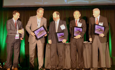
Awards from the SPIE Advanced Lithography Symposium
Here is a recap of the various people who were recognized with awards at this year’s SPIE Advanced Lithography Symposium. (photos by SPIE, http://spie.org/x112637.xml)
Career Achievement Award
Andy Neureuther and Bill Oldham were acknowledged for their “career long contribution to the art and science of lithography.” The award was made “in deep appreciation for your 40 years of visionary guidance and dedication to SPIE society and lithography community.”

12th Frits Zernike Award
Ralph Dammel, CTO of AZ Electronic Materials

Fellows of SPIE
Luigi Capodieci, Bernd Geh, Moshe Preil, Masato Shibuya, and Obert Wood
From the Metrology conference:
Diana Nyyssonen Award for Best Paper in Metrology (2014 conference):
“10nm three-dimensional CD-SEM metrology”, András E. Vladár, John S. Villarrubia, Jasmeet S. Chawla, et al.,
Karel Urbanek Award for Best Student Paper (student lead author at this year’s conference):
“Mechanical and thermal properties of nanomaterials at sub-50nm dimensions characterized using coherent EUV beams”, Kathleen M. Hoogeboom-Pot, Jorge N. Hernandez-Charpak, Travis Frazer, Xiaokun Gu, Emrah Turgut, Univ. of Colorado at Boulder; Erik H. Anderson, Weilun L. Chao, Lawrence Berkeley National Lab.; Justin M. Shaw, National Institute of Standards and Technology; Ronggui Yang, Margaret M. Murnane, Henry C. Kapteyn, Damiano Nardi, Univ. of Colorado at Boulder
From the Patterning Materials conference:
C. Grant Willson Best Paper Award (2014 conference):
“EUV Resists based on Tin-Oxo Clusters”, Brian Cardineau, Ryan Del Re, Hashim Al-Mashat, Miles Marnell, Michaela Vockenhuber, Yasin Ekinci, Chandra Sarma, Mark Neisser, Daniel A. Freedman, and Robert L. Brainard
Hiroshi Ito Memorial Award for the Best Student Paper (2014 conference):
“An insitu hard mask block copolymer approach for the fabrication of ordered, large scale, horizontally aligned, Si nanowire arrays on Si substrate”, Tandra Ghoshal, Ramsankar Senthamaraikannan, Matthew T. Shaw, Justin D. Holmes and Michael A. Morris
Jeffrey Byers Memorial Best Poster Award (2015 conference):
“EUV Resists Comprised of Main Group Organometallic Oligomeric Materials”, James Passarelli, Brian Cardineau, Ryan Del Re, Miriam Sortland, Michaela Vockenhuber, Yasin Ekinci, Chandra Sarma, Mark Neisser, Daniel A. Freedman, and Robert L. Brainard
From the Design Process Technology Co-Optimization conference:
First Annual Franco Cerrina Memorial Best Student Paper Award (2015 conference):
“Toplogy and context-based pattern extraction using line-segment Voronoi diagram”, Sandeep K. Dey, Univ. della Svizzera Italiana (Switzerland)
From the Optical Lithography conference:
Cymer Best Student Paper Award (2015 conference):
“Characterizing the dependence of thick-mask edge effects on feature size and illumination angle using AIMS images” Aamod Shanker, Andrew R. Neureuther, Laura Waller, Univ. of California, Berkeley; Martin Sczyrba, Advanced Mask Technology Ctr.; Brid Connolly, Toppan Photomasks
350 Years of Scientific Journals
On March 6, 1665 something quite special happened. It probably didn’t seem that special at the time, but the publication of the first issue of the Philosophical Transactions in London created a vital communication tool in science: the scientific journal. 350 years later that journal is still being published, joined by tens of thousands of other scientific journals that chronicle and transmit that vital currency of science: knowledge.
I recently wrote a short article on the 350 history of scientific journals. If you are interest, you can find it here.
SPIE Advanced Lithography Epilogue
I gave three talks at last week’s SPIE Advanced Lithography Symposium, and I’ve spent a fair part of this week finishing up the papers. I am happy to say that they are all now complete. As usual, they are available for download for anyone interested.
But I’ve done something different this year. I have, after the fact, recorded my presentations and uploaded them to YouTube. So, for anyone who missed my presentations and wants to hear what I have to say, you can find both the written papers and the talks here:
SPIE Advanced Lithography 2015 – day 2
It’s been a long time since a lithography conference was just about lithography. Last year TSMC gave a talk that described problems they were having with EUV lithography and ASML’s stock price went down 5%. Yesterday (Monday), Tony Yen of TSMC gave a talk describing very nice progress on source power and throughput and ASML’s stock price went up 5%. Is it a good thing that so many stock analysts attend these talks? It doesn’t help that ASML had a press release ready to go and sent it out just minutes after Tony had finished (Title: “ASML announces new high mark for EUV productivity; TSMC images more than 1000 wafers in a single day”). About half a dozen analyst blogs were crowing about the importance of what Tony said, one even counting the number of times he mentioned KLA-Tencor. This puts a lot of pressure on scientists and engineers giving technical talks to focus on things that aren’t technical, and that is pressure we do not want or need. I guess there is nothing to be done – it is just reality. But I don’t like it.
My Tuesday was far from such earth-shaking events. I buried myself deep in the rough landscape of stochastic resist response, line-edge roughness (LER), and how to measure noise. Fascinating, but don’t expect a stock analyst to be parsing any of my words on the topic. There were several attempts to simulate the impact of roughness on SEM linewidth measurement, with important insights. Richard Lawson of Georgia Tech showed that roughness on a vertical feature sidewall produces SEM images that look just like smooth sidewalls that are sloped. There is a lot of information in an SEM image, but maybe less than we hope. My 8am paper was about how to extract the most information possible from an SEM image, and that our current measurement algorithms don’t take advantage of everything we know about how those images are generated. As I said Monday night, build better metrology. We desperately need it.
My third and last paper was Tuesday afternoon, where I gave a mathematical proof that post-lithography process smoothing techniques won’t work, at least not as well as we need them to. Like all mathematical proofs, its validity will depend on the validity of my assumptions. I hope that those who believe in the efficacy of post-process smoothing will design experiments that directly challenge those assumptions instead of just showing SEM images and reporting reduced three-sigma roughness numbers.
The conference is half-way done!
SPIE Advanced Lithography 2014 – day 1
If you walk through the crowds this year, you know the symposium is well attended. We have about 50 less papers this year than last, but about the same number of attendees – on the order of 1,700 technical attendees and another 800 or so who just come to the exhibits. Short course attendance was up about 25% from last year. A very healthy and dynamic conference.
We began our first day with the awards ceremony, and a very rare “career achievement” award. Andy Neureuther and Bill Oldham were acknowledged for their “career long contribution to the art and science of lithography” through their lithography modeling efforts at the University of California at Berkeley. Andy was a co-author of some of the original 1975 Dill papers (the most famous papers in lithography, in my opinion) and Andy and Bill, along with their students, published the SAMPLE simulator in 1979. Their SAMPLE group made numerous important contributions to lithography over the last 35 years, and of course the many great students they have graduated continue to multiply their influence. As Symposium Chair Mircea Dusa said, this work was a “defining moment, when lithography went from an art to a science.” The award was made “in deep appreciation for your 40 years of visionary guidance and dedication to SPIE society and lithography community.” Congratulations Andy and Bill!
Ralph Dammel, CTO of AZ Electronic Materials, was the recipient of the 12th Frits Zernike award (full disclosure – I nominated him). I learned a tremendous amount from Ralph’s 1993 book on DNQ/Novolac resists, and learned to appreciate sweetbreads and German coffee when I visited him in Frankfurt about 25 years ago. A well-deserved award (for the lithography, not the sweetbreads).
We have five new Fellows of SPIE in our community as of Monday: Luigi Capodieci, Bernd Geh, Moshe Preil, Masato Shibuya, and Obert Wood. GlobalFoundries almost swept the ranks! Congratulations to all of you.
The plenary session was a mixed bag. Alan Willner gave a nice overview of the National Photonics Initiative, an “alliance” of industry, academia, and government that includes SPIE and that began in 2012. The goal of the NPI is to drive US investment in photonics (read: get the US government to spend more on photonics). Photonics, like many fields of science that border technology, seems to have a case of Moore’s Law envy.
The talk by Tsu-Jae King Liu of UC Berkeley was one of the best plenaries ever. With power as the current limiter of CMOS performance scaling, she proposed a couple of very innovative solutions. The use of micro-relays was especially intriguing. I’ll be following developments in that field going forward.
I have been out of corporate America too long to appreciate Xiaowei Shen’s final plenary talk on the “internet of things”. It was so full of IBM-speak that I could barely understand it.
When the regular conference talks began at 11am I had the familiar problem of wanting to be in multiple places at the same time. I missed more worthy talks than I attended. Gerg Yeric of ARM showed me how little I know about design-manufacturing interactions and how hard scaling is getting independent of lithography. He noted that when we shrink, some of the SRAM cells in logic designs are moving from 6 transistors to 8, 10, or even 18 transistors to store one bit in order to keep the cells both fast and reliable in the face of variability. It makes you wonder if cost per transistor is a useful metric to assess the value of shrinking.
Changmoon Lim of SK hynix gave a talk on challenges for EUV insertion into high-volume manufacturing (HVM), a perennial topic at this conference. The Hynix experience on the NXE:3100 EUV tool from ASML was about slow learning. The tool was installed in the summer of 2011 and over three years the throughput went from 2 wafers per hour (WPH) to 7 WPH, and tool availability went from 25% to 75%. Learning is picking up with the installation of their NXE:3300, though he gave little data. A 2xnm generation DRAM split lot with one layer printed on EUV produced comparable yield to 193i, but they had to use an exposure dose much higher than the goal of 20 mJ/cm2 to achieve that yield (when I asked, he wouldn’t tell me the exact dose used).
I missed Tony Yen’s talk about EUV progress at TSMC – I was busy giving a talk of my own. I’m told he described the very fast progress that source power has made in the last year, going from 20W to 40W, and more recently to 80W, installed on a TSMC tool. I also missed Todd Younkin of Intel and the idea of bottoms-up growth of metal vias next to cuts filled with dielectric to improve overlay. He told me later than much work remains on this idea, but it sounds very promising.
Toshiaki Ikoma, CTO of Canon, gave an overview of their new nanoimprint lithography (NIL) tool, claiming the tool was “now available” and that Canon “will be back to the leading lithography company again.” We’ll have to wait and see. And we’ll have to wait to see the data that support these claims during other NIL talks this week.
The day ended with a panel discussion on the metrology challenges of 3D devices. I was on the panel, but since I know nothing about the metrology challenges of 3D devices, I gave a speech on a different topic. You can find my speech here: http://www.lithoguru.com/scientist/essays/Metrology.html.
A general complaint about panel discussions: the standard format that we almost always use doesn’t work. We should abandon it. This format involves posing a number of momentous and difficult questions, and telling each panelist to prepare a 5 minute talk on those questions. Of course, the panelists use powerpoints (most of us are barely able to talk without powerpoint, and I suspect the audience is barely able to listen without powerpoint as well), and each one averages 10 minutes. Our scheduled 90 minute panel had only 30 minutes of audience questions at the end, but that was only because we went 20 minutes over the allotted time. Through no fault of the fine panelists on stage with me, it was a truly boring experience. How can we make panels better? Give the panelists at most one minute (and no slides) to make an introductory statement, or better yet no introductory statement. Then go right into questions, alternating between moderator and audience questions. Make sure it is fun, and not a mini conference session. Also, beer helps.
My favorite quote of the day: “Double patterning was thought to be a bridge between immersion and EUV, we just didn’t realize how long the bridge would be.” – Changmoon Lim, SK hynix