Tag Archives: Mircrolithography

SPIE Advanced Lithography and Patterning Symposium 2023 – day 2

(This post is certified ChatGPT-free.)

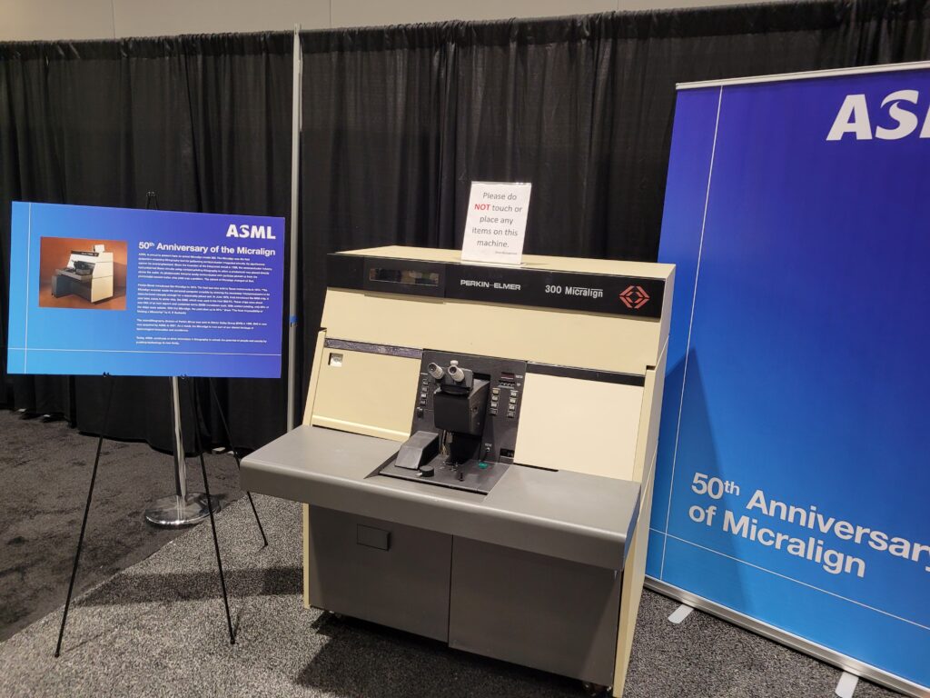
The day began with a second plenary, starting with ASML/SVGL/Perkin-Elmer veteran Chip Mason describing the history of the first commercial projection lithography tool, the Micralign, on the occasion of its 50th birthday.  I am very sorry to say that another commitment prevented me from attending Chip’s talk, but numerous people (young and old) told me that it was fantastic.  My first job as a lithographer (exactly 40 years ago this month!) involved supporting a fab with both a Micralign 300 and an Optimetrix 10X stepper, so the importance of the Micralign is also a bit personal for me.  (Steppers were introduced five years later, in 1978, but the Micralign remained the workhorse of the industry well into the 1980s.)  But not only did we hear about the Micralign, we get to see one.  ASML now owns the former Perkin-Elmer site in Wilton, Connecticut where the Micralign was developed and manufactured, and they managed to find a Micralign in a garage somewhere (Vermont, I believe).  The owner donated the tool and ASML had it shipped to San Jose where it is now on display (for one more day) in the Exhibitors’ Hall.  Seeing a Micralign 300 in person is a wonderful opportunity.

Micralign 300 by Perkin-Elmer
Micralign 300 by Perkin-Elmer on display at the SPIE Advanced Lithography and Patterning Symposium

Attending papers on Tuesday morning had me bouncing between sessions, as usual.  Rudy Peeters of ASML gave an update on the readiness of high-NA EUV tools, including the status of the the four major components of the tool (source, reticle stage, wafer stage, and projection optics).  Three EXE:5000 sources have been qualified (benefiting from commonality with sources from the low-NA tool), four wafer stages have been built (and are working towards testing at full acceleration), and one reticle module was built and is being tested.  Multiple mirrors have been made, and so the next major milestone to watch for will be the first working projection optics box.  It is fun to hear ASML express their optimism as if it were established fact:  the goal of the high-NA EUV tool introduction in 2025 is to “replace EUV double patterning.”  It is also interesting to infer the market ambiguity of this tool from statements like “high contrast imaging can be used for better images or better dose.”

Greg Denbeaux of SUNY Polytechnic (Albany) gave a very nice talk on attempts to move the idea of polymer aggregation as a source of resist stochastic variability from speculation to experimental measurement.  By printing an open-frame EUV exposure at the dose to clear, residual resist at the substrate can be measured with an AFM to get some feeling of the size of the clumps of resist there.  I wouldn’t call the method exactly quantitative, but it is a start.

Yaniv Abramovitz of AMAT looked at using in-device overlay measurement by a SEM at ADI (after develop inspect) rather than the traditional AEI (after etch inspect) measurements, and compared them to optical scribe-line measurements.  His results from the classical skew experiment (where the scanner is directed to purposely offset the stage position of the second layer in increments, and then the measured overlay is plotted versus this scanner input skew) yielded unexpected slopes far less than 1.  How could this be?  Scanners have incredibly accurate stage positioning.  AMAT has some more work to do.

Overlay and the role of stochastics in edge placement error (EPE) is my new special interest, so I spent the rest of the morning and much of the afternoon in sessions on those topics.  Myungjun Lee of Samsung gave a fascinating talk on their development of hyper spectral imaging reflectometry for massive overlay and CD measurements.  The traditional OCD (optical CD) approach collects reflected spectrum (reflectivity versus wavelength at a fixed angle) using a modest spot size (20 – 100 microns) aimed at a target of regular patterns (usually lines and spaces of fixed pitch).  Analysis of the spectrum yields measurement of the CD, and possibly other information about the features.  Spectral “imaging” reflectometry shrinks the spot size (to about 5 microns in this case) and uses that spot as one pixel in a larger “image” of many pixels.  It is only an image in the sense that imaging optics are uses to collect data from each pixel in parallel, so that this technique is essentially massively parallel OCD.  How massive?  3200 x 3200 pixels covering a 20.8 mm x 20.8 mm field.  The massive data that can result from this tool opens up many interesting use cases.  It is my understanding that Samsung is looking for an equipment partner to commercialize the technology.

Several authors (starting with myself the day before) described how EPE measurements are best used as an input to a calculation of yield (or number of good die).  Inho Kwak of Samsung showed that using a prediction of number of good die (generically called a KPI = key process index, in the jargon of the fab) during advanced process control (APC) resulted in a 5% improvement of dies in spec.  The control strategy first suggests an adjustment of the dose of the second layer, then calculates the overlay correctables to achieve lowest EPE (rather than individually trying to match CD with dose, then overlay with the correctables).  Harm Dillen of ASML and Franz Zach of KLA proposed similar approaches.

In the SEM measurements session I especially like John Villarrubia’s talk on three new SEM-based fundamental research projects at NIST.  John is the author of a standard Monte Carlo simulator for SEM behavior called JMONSEL, and these new projects aim to fill in some gaps and improve the accuracy of this simulator.  The first experimental piece will compare a top-down SEM image at low voltage to a STEM (scanning transmission electron microscopy) image at high voltage for the same sample and in the same instrument.  The second experiment measures secondary electron yield of materials, with the benefit that the materials are deposited and then measured without exposing the films to the atmosphere.  The third project seeks to improve the models in JMONSEL using the data from the first two projects.  This is a very worthwhile activity, and I commend John and NIST for taking a leadership role in these investigations.

The last talk I attended was also one for which I was a coauthor.  Genevieve Kane of IBM gave her first SPIE presentation – congratulations on a nice job!

SPIE Advanced Lithography and Patterning Symposium 2023 – day 1

The plenary session Monday morning began with awards.  I was glad to hear that 27 students received grants from SPIE to cover their registration and travel to the conference (Fractilia is one of the corporate sponsors of these student grants and I was happy to meet some of those students later that day at a student-mentor lunch).  Tony Yen of ASML was this year’s winner of the Frits Zernike Award for Microlithography – congratulations!  The Kingslake Award for Optical Design is not usually presented at this conference, but this year’s winner Wilhelm Ulrich chose to receive that honor here since his work at Zeiss in designing lithographic lenses was the reason for this prestigious reward.

Was saw eight new SPIE fellows from our community inducted this year, seven of whom were on hand to be recognized for this achievement: Martin Burkhardt of IBM, Debbie Gustafson of Energetiq, Larry Melvin of Synopsis, Warren Montgomery of EMD Electronics, Linyong Pang of D2S, Takashi Sato of KIOXIA, Geert Vandenberghe of imec, and Yayi Wei of the Chinese Institute of Microelectronics.  A great group of fellows, indeed.

As I glanced back across the room before the start of the first plenary talk, I was gratified to see what once was a familiar site:  the largest lecture hall at the San Jose convention center was full to overcrowding, standing room only, with an overflow room set up to accommodate the rest.  We are back!  And our first plenary speaker of the day, Martin van den Brink of ASML, did not disappoint in a talk densely packed with interesting information.  Martin gave a plenary speech 15 years earlier where he projected scaling for the coming 15 years, so it was fun to hear him compare those projections to reality (he did better than most prognosticators) and then try it again, providing ASML’s vision of Moore’s Law in the coming decade.  Of course, he predicted lithography scaling would continue – it is in ASML’s DNA (and I suspect in their corporate bylaws as well).

Martin described the well-known evolution of Moore’s Law away from transistor scaling towards system scaling, especially for energy efficient performance (EEP).  Still, he remains hopeful that DRAM scaling will continue down to 15 nm pitch, and vertical NAND flash will grow to 1000 transistors tall!  ASML is pushing massive e-beam inspection to approach optical defect inspection in terms of productivity, a tough road, but I am sure they will be at least partially successful.  I was almost numbed to see projections of DUV scanner throughput to 400 wafers per hour, and even 500 wph!  My first thought was “that’s impossible”, but I’ve come to understand that these kinds of things are impossible only until ASML does them.  Of course sustainability is on everyone’s mind nowadays, so Martin addressed the 100 kW-hour per finished wafer energy expenditure for lithography.  The goal is for that number to at least remain the same, if not go down over time.  As for EUV source power, 500W is said to be on the way, 600W is being demonstrated, and 800W is on the roadmap.  Each increase is EUV source power is of course very challenging.

Maybe the most interesting part of his talk (at least for me) was the new optical designs that removed one mirror from both the 0.33 and 0.55 NA systems (from the illuminator, it appeared).  Since each mirror has less than 70% reflectivity, the removal of one mirror represents a significant throughput advantage for these EUV scanners. He also described ASML’s plans for EUV “hyper” NA, a 0.75 NA design.  But without polarization (which Martin admitted would not happen), the image contrast benefit of the higher NA is reduced, so that a cost/benefit analysis of hyper-NA EUV seems clearly against it ever becoming a reality.  Time will tell, but of course ASML must have a roadmap.

I did not stick around for the second plenary talk on the Chips Act (I’m not going to apply for any of that money), so it was off to the regular conference papers.  Martin Weiss of Intel talked about modeling the matching of high-NA EUV two-field to low-NA one field difficulties.  It seems Intel is still hoping to jump back into the lead in scaling by being the first to implement high-NA EUV into production.  Good luck to them – that is going to be very hard, and probably late.  Zhigang Wang and B.H. Lee of Hitachi High Technology talked on the future of CD-SEM metrology, emphasizing the need for 0.01 nm tool-to-tool matching (or at least of that order) without giving much of a hint how they might achieve that.  I agree with them that SEM tool matching needs significantly more attention.  Ryosuke Kizu of the National Metrology Institute of Japan gave another good paper this year on their metrological tilt-AFM tool.  This year they looked at how SEM exposure of resist results in sidewall roughness smoothing – an important topic for those of us trying to measure resist feature roughness using top-down CD-SEMs.  I hope Kizu can partner with a CD-SEM owner to turn this interesting experimental technique into results useful to semiconductor metrologists.

In the EUV+Optical/Resist joint session in the afternoon there were a pair of papers by FujiFILM followed by Samsung looking at developer and rinse effects on line-edge roughness.  Both seemed to indicate that NTD (negative tone develop) using solvent developer for EUV held some promise for roughness and defect reduction, but I would consider these results preliminary at best.  I hope they work with imec to validate this behavior.

While there were a few other good papers late in the afternoon, my business obligations prevented me from attending them.  I had to go to the Fractilia Happy Hour at Uproar Brewing.  Ah, the burdens of entrepreneurship.

SPIE Advanced Lithography and Patterning Symposium 2023 – day 0

It looks like we are back to normal.  After three years where Covid 19 was on everyone’s minds and tongues (if not yet in the upper respiratory tracts), today more people seem interested in snow on the mountains surrounding San Jose, the massive downtown in the memory business, the nasty weather outside, and who survived the layoffs at company xyz.  Different is the new normal.  It is good to be back!

The conference itself is back to its former vigor.  Compared to 2019, submissions are up (over 450), attendance is about the same (over 2000 seems likely), and the number of exhibitors is about the same (a low 54).  I had 11 people in my all-day short course on Sunday (lower than hoped, but a great group!).  And the reconnecting with friends has already begun. From a technology perspective, what will the week be like?  I have to admit that I am completely clueless.  I haven’t yet dived into the agenda of talks (I miss the printed programs), and only know that I need to be at the plenary program at 8am on Monday.  My one talk is Monday at 2:30pm, and the Fractilia Happy Hour is also Monday, so that day is my current focus (I’ll think about Tuesday on Tuesday).  And so another week at ALP begins…

SPIE Advanced Lithography Symposium 2016 – a prologue

2016 will prove to be a pivotal year in the history of semiconductor lithography.  How do I know this?  Because every year proves to be a pivotal year in the history of lithography.  Why should 2016 be any different?  Our industry moves too fast to allow a slack year.

I am frequently reminded of Sturtevant’s Law, not just because it is cute and funny (though it is), but because behind the humor lies a profound truth.  Sturtevant’s Law says that the end of optical lithography is 6 – 7 years away.  Always has been, always will be.  When I started in the field of lithography way back in 1983, Sturtevant’s Law was as yet unformulated but nonetheless in full swing.  X-ray or e-beam lithography was sure to take over by 1990 since it was obvious that optical lithography could not cross the 1 micron barrier.

This was but one of many, many failed predictions of the end of optical lithography.  But the fundamental truth behind Sturtevant’s Law is this:  we always know what we are doing for the next node (in 2 – 3 years), and are pretty sure about the node after that, but we have almost no visibility into what comes next.  We know all of the unsolved problems looming beyond the 6 year horizon, and can’t quite picture the solutions.  Sturtevant’s Law is a statement about our research and development timelines and how they relate to the pace of Moore’s Law.

But while Sturtevant’s Law has been in force for over 30 years, I’m afraid that it may be coming to an untimely end.  The reason is simple:  we no longer have good visibility out to two nodes (6 years).  We have a just barely reasonable impression about what the next node will bring, and are sure that the node after that is impossible.  The end of optical lithography is no longer 6 -7 years away, it is 2 – 3 years away, and even that time frame seems impossibly distant and opaque.

Our angst is about more than just lithography.  Of course, we lithographers know that the industry moves to the pace that we set.  Still, it is disconcerting to believe that a slowdown in lithography means the end of Moore’s Law.  Yet that is what is at stake.  In 2016, we must discover a path that keeps Moore’s Law moving forward, or watch Moore’s Law fall flat.

But a slowdown of Moore’s Law has already begun.  Intel’s 14-nm node was a year late, and Intel has admitted that its 10-nm node will also be late, on a 3-year node pace rather than the historic 2-year cycle.  TSMC has not admitted the slow-down, but is experiencing it anyway.  They created a “faux” node, a 16-nm product line that has the same dimensions and density as the previous 20-nm node.  Revealingly, when the 16-nm node came online last year, they did not report the revenues of that node separately as had been their normal practice, but rather began to lump the 16 and 20-nm node revenues together in one bucket.  “Follow the money” was good advice coming from Deep Throat, and is good advice in the semiconductor industry as well.

Moore’s Law is slowing down because lithography is not keeping up.  Multiple patterning is expensive and process control is a serious problem.  No other solutions are available.  Now, this where EUV is supposed to come in and save the day, right?

Alas, EUV is late.  ASML has made very good progress in the last two years, but that progress has been enough to keep EUV late, not enough to catch up with the industry need.  Anyone who has read these conference blogs before knows that I have been and continue to be an EUV skeptic.  But for the first time in over 20 years of development, I finally see a glimmer of hope for EUV.

Time is the enemy of all lithography development programs.  The demands of lithography move at an unrelenting pace, and even the slightest schedule slip in a lithography development program is the kiss of death.  EUV is late, an almost unmistakable sign of failure, and yet finally there is hope.  And here is the reason.

EUV was supposed to save Moore’s Law.  But instead, the slowdown of Moore’s Law may save EUV.

The 10-nm node will be two years late compared to the original schedule (naming games aside), as we are now on a three-year Moore’s Law cycle.  But since EUV is more than two years late, it still could not impact that node.  How late will the 7-nm node be?  Could it be late enough to use EUV?  That is a distinct possibility.

The big picture of lithography is bigger than the picture we will see at the SPIE Advanced Lithography Symposium in 2016, since the big picture involves the macroeconomics of the semiconductor industry itself.  But what we will see here this week is still big and very important.  How painful is multiple patterning really?  How close is directed self-assembly to being production worthy?  What is the status of nanoimprint manufacturing for Flash production?  Has there been any progress in taming the roughness beast?  And of course, what about EUV source power?

There are always many questions coming into the start of the SPIE lithography conference.  I am excited to start learning the answers.